图5-20/Q分频器仿真波形… 60 V
V 图 5-20 I/Q 分频器仿真波形··························································· 60
表目录 表3-1鉴频鉴相器的工作模式 27 表5-1/Q分频器后仿结果…60 VII
VII 表目录 表 3-1 鉴频鉴相器的工作模式 ························································ 27 表 5-1 I/Q 分频器后仿结果 ···························································· 60

摘要 本论文围绕△Σ分数分频频率综合器的设计展开,主要包括鉴频鉴相器、电 荷泵、分频器以及Q分频器等电路模块的设计。该频率综合器应用于一款 CMOS全集成直接变频结构的数字电视调谐器芯片。为了把VHF/UHF频段上的 数字电视信号下变频到零中频,需要其提供48~869MHz的正交本振信号。因此, 该频率综合器对频率范围及信噪比有着较高要求,这也给电路的设计带来了诸多 挑战。 首先,论文对频率综合器做了概述,介绍了基于锁相环的分数分频频率综合 器的几个关键性能指标,并且总结了频率综合器的设计流程。这对具体电路的设 计具有指导意义。 其次,论文详细讨论了频率综合器中几个模块的设计。针对电荷泵型鉴频鉴 相器的非线性特性,本文提出了一种降低非线性的技术,来减小鉴频鉴相器和电 荷泵对带内噪声的贡献。针对全差分电荷泵复杂的电路结构,本文采用源端开关 型电荷泵单元,从而简化了电路,并且使得电荷泵上下电流的调节来得更为简单。 在Q分频器的设计中,本文采用CML结构的除二分频器来满足电路对正交匹 配特性的较高要求,并且通过引入一个对输入信号放大整形的电路,很好地解决 了困扰电路的灵敏度问题。 最后,给出了相应电路模块的版图以及仿真结果,验证了电路功能的正确性。 本文参与设计的频率综合器在TSMC的0.18um的工艺下成功流片,频率范围 覆盖0.8GHz~1.8GHz,总的芯片面积为0.9mm×0.9mm。其中鉴频鉴相器和电 荷泵的功耗为1.4mA,4/5预分频器的功耗为1.2mA,I/Q分频器的功耗为 4~6mA。环路滤波器的带宽为75kHz。I/Q分频器的正交相位误差小于0.5°。带 内相位噪声低于-100dBc/Hz。锁定时间小于30μs。 关键词:电视接收机,频率综合器,鉴频鉴相器,全差分电荷泵,线性化技术, I/Q分频器,4/5预分频器,相位噪声 中文分类号:TN4
IX 摘要 本论文围绕 ∆Σ 分数分频频率综合器的设计展开,主要包括鉴频鉴相器、电 荷泵、分频器以及 I/Q 分频器等电路模块的设计。该频率综合器应用于一款 CMOS 全集成直接变频结构的数字电视调谐器芯片。为了把 VHF/UHF 频段上的 数字电视信号下变频到零中频,需要其提供 48~869MHz 的正交本振信号。因此, 该频率综合器对频率范围及信噪比有着较高要求,这也给电路的设计带来了诸多 挑战。 首先,论文对频率综合器做了概述,介绍了基于锁相环的分数分频频率综合 器的几个关键性能指标,并且总结了频率综合器的设计流程。这对具体电路的设 计具有指导意义。 其次,论文详细讨论了频率综合器中几个模块的设计。针对电荷泵型鉴频鉴 相器的非线性特性,本文提出了一种降低非线性的技术,来减小鉴频鉴相器和电 荷泵对带内噪声的贡献。针对全差分电荷泵复杂的电路结构,本文采用源端开关 型电荷泵单元,从而简化了电路,并且使得电荷泵上下电流的调节来得更为简单。 在 I/Q 分频器的设计中,本文采用 CML 结构的除二分频器来满足电路对正交匹 配特性的较高要求,并且通过引入一个对输入信号放大整形的电路,很好地解决 了困扰电路的灵敏度问题。 最后,给出了相应电路模块的版图以及仿真结果,验证了电路功能的正确性。 本文参与设计的频率综合器在 TSMC 的 0.18m 的工艺下成功流片,频率范围 覆盖 0.8GHz~1.8GHz,总的芯片面积为 0.9mm×0.9mm。其中鉴频鉴相器和电 荷泵的功耗为 1.4mA,4/5 预分频器的功耗为 1.2mA,I/Q 分频器的功耗为 4~6mA。环路滤波器的带宽为 75kHz。I/Q 分频器的正交相位误差小于 0.5˚。带 内相位噪声低于-100dBc/Hz。锁定时间小于 30s。 关键词:电视接收机,频率综合器,鉴频鉴相器,全差分电荷泵,线性化技术, I/Q 分频器,4/5 预分频器,相位噪声 中文分类号:TN4
Abstract This thesis takes efforts on the design of aA>fractional frequency synthesizer,including phase detector,charge pump,divider and I/Q divider blocks.Applied to a CMOS fully integrated conversion structure of the digital TV tuner,the frequency synthesizer should generate a quadrature local oscillator signal ranging from 48MHz to 869MHz,which used to the conversion of the UHFNVHF band frequency to zero IF.Inevitably,some challenges are invited for high requirements,such as the wide frequency range,the high SNR, etc. Firstly,this thesis presents a review of the frequency synthesizer,which of described three main fundamental figures of merit,and it concludes the process of the frequency synthesizer design.All over the work will be instructive. Secondly,this thesis is mainly dedicated to the analysis and the design of four modules:phase detector,charge pump,divider and l/Q divider circuits.In terms of PFD/CP nonlinearity,a linearization technology was proposed to alleviate the contribution of PFD phase noise inband;In terms of the complexity of the fully differential charge pump,the core unit of charge pump is redesigned for simplification,also with regulating current mismatch easier;In terms of high requirement on the quadrature characteristic,circuits and layout work are coordinated to optimize the design;And also,a variation on the structure of I/Q divider was adopted,taking into account the sensitivity and the power requirements. Finally,thanks to the other colleagues'work,including voltage controlled oscillator,loop controlled blocks etc.,a 0.8GHz~1.8GHz AZ fractional frequency synthesizer was implemented in TSMC 0.18-um process successfully.The chip area is 0.81mm2;and the PFD/CP power is 1.4mA,the 4/5 prescaler power is 1.5mA,the l/Q divider power changed along with frequency and divided ratio is about 4~6mA;the inband noise is below -100dBc/Hz;the bandwith of loop fliter is 75kHz;the quadrature phase error is under0.5°;the locking time is less than30us. Key Words:Television Receiver;Frequency Synthesizer;Phase Frequency Detector:A Fully Differential Charge Pump;Linearization Technique;l/Q Divider;4/5 Prescaler;Phase Noise XⅫ
XI Abstract This thesis takes efforts on the design of a ∆Ʃ fractional frequency synthesizer, including phase detector, charge pump, divider and I/Q divider blocks. Applied to a CMOS fully integrated conversion structure of the digital TV tuner, the frequency synthesizer should generate a quadrature local oscillator signal ranging from 48MHz to 869MHz, which used to the conversion of the UHF/VHF band frequency to zero IF. Inevitably, some challenges are invited for high requirements, such as the wide frequency range, the high SNR, etc. Firstly, this thesis presents a review of the frequency synthesizer, which of described three main fundamental figures of merit, and it concludes the process of the frequency synthesizer design. All over the work will be instructive. Secondly, this thesis is mainly dedicated to the analysis and the design of four modules: phase detector, charge pump, divider and I/Q divider circuits. In terms of PFD/CP nonlinearity, a linearization technology was proposed to alleviate the contribution of PFD phase noise inband; In terms of the complexity of the fully differential charge pump, the core unit of charge pump is redesigned for simplification, also with regulating current mismatch easier; In terms of high requirement on the quadrature characteristic, circuits and layout work are coordinated to optimize the design; And also, a variation on the structure of I/Q divider was adopted, taking into account the sensitivity and the power requirements. Finally, thanks to the other colleagues’ work, including voltage controlled oscillator, loop controlled blocks etc., a 0.8GHz~1.8GHz ∆Ʃ fractional frequency synthesizer was implemented in TSMC 0.18-m process successfully. The chip area is 0.81mm2 ; and the PFD/CP power is 1.4mA, the 4/5 prescaler power is 1.5mA, the I/Q divider power changed along with frequency and divided ratio is about 4~6mA; the inband noise is below -100dBc/Hz ; the bandwith of loop fliter is 75kHz; the quadrature phase error is under 0.5˚; the locking time is less than 30s. Key Words: Television Receiver; Frequency Synthesizer; Phase Frequency Detector; A Fully Differential Charge Pump; Linearization Technique; I/Q Divider; 4/5 Prescaler; Phase Noise
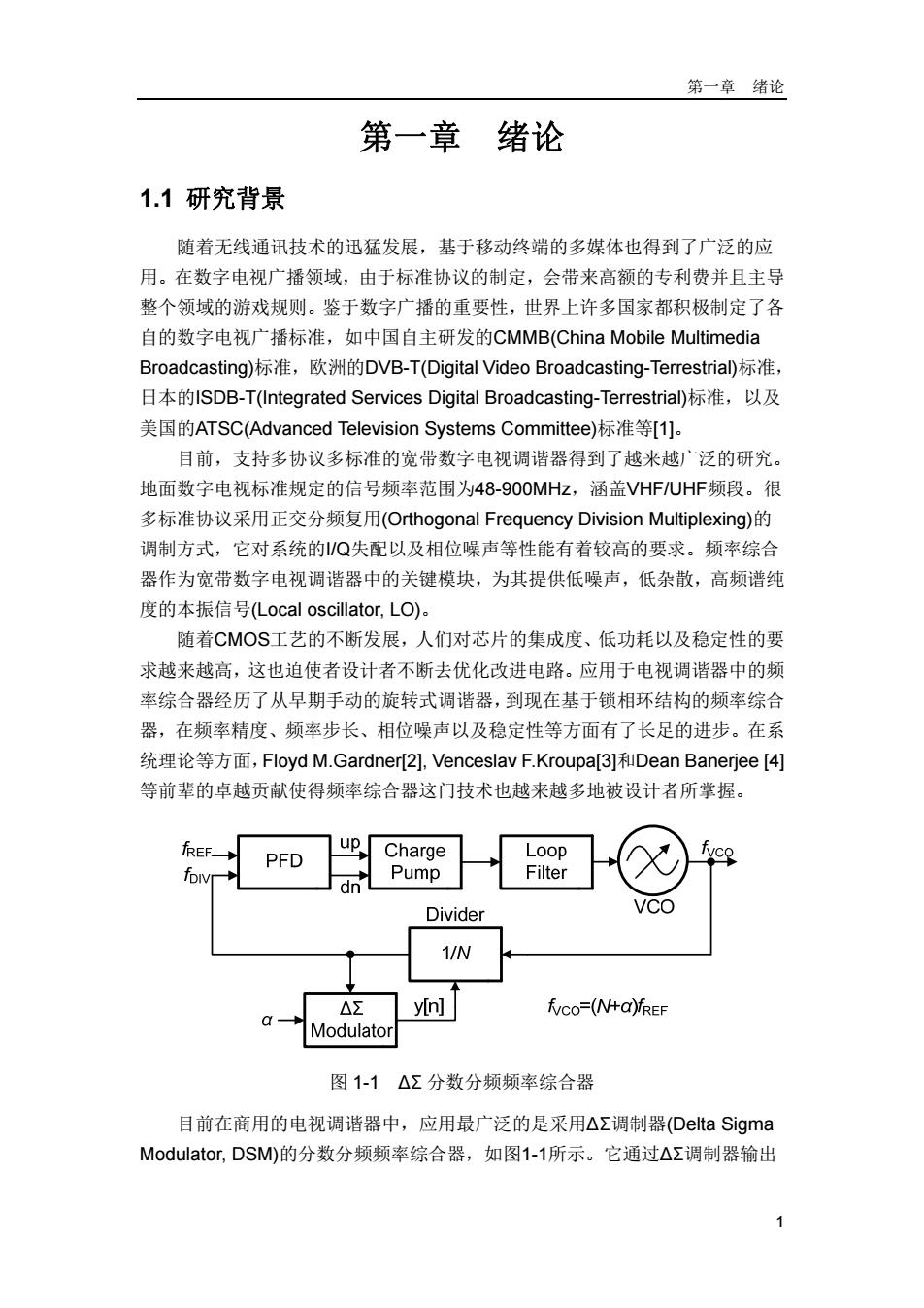
第一章绪论 第一章绪论 1.1研究背景 随着无线通讯技术的迅猛发展,基于移动终端的多媒体也得到了广泛的应 用。在数字电视广播领域,由于标准协议的制定,会带来高额的专利费并且主导 整个领域的游戏规则。鉴于数字广播的重要性,世界上许多国家都积极制定了各 自的数字电视广播标准,如中国自主研发的CMMB(China Mobile Multimedia Broadcasting)标准,欧洲的DVB-T(Digital Video Broadcasting-Terrestrial标准, 日本的SDB-T(Integrated Services Digital Broadcasting-Terrestrial)标准,以及 美国的ATSC(Advanced Television Systems Committee)标准等[1]。 目前,支持多协议多标准的宽带数字电视调谐器得到了越来越广泛的研究。 地面数字电视标准规定的信号频率范围为48-900MHz,涵盖VHF/UHF频段。很 多标准协议采用正交分频复用(Orthogonal Frequency Division Multiplexing)的 调制方式,它对系统的Q失配以及相位噪声等性能有着较高的要求。频率综合 器作为宽带数字电视调谐器中的关键模块,为其提供低噪声,低杂散,高频谱纯 度的本振信号(Local oscillator,,LO). 随着CMOS工艺的不断发展,人们对芯片的集成度、低功耗以及稳定性的要 求越来越高,这也迫使者设计者不断去优化改进电路。应用于电视调谐器中的频 率综合器经历了从早期手动的旋转式调谐器,到现在基于锁相环结构的频率综合 器,在频率精度、频率步长、相位噪声以及稳定性等方面有了长足的进步。在系 统理论等方面,Floyd M.Gardner[2],Venceslav F.Kroupa[3]和Dean Banerjee[4] 等前辈的卓越贡献使得频率综合器这门技术也越来越多地被设计者所掌握。 fREF- up PFD Charge Loop Pump Filter dn Divider 1/N △∑ yIn] fyco=(N+a)fREF Modulator 图1-1△Σ分数分频频率综合器 目前在商用的电视调谐器中,应用最广泛的是采用△Σ调制器(Delta Sigma Modulator,DSM)的分数分频频率综合器,如图1-1所示。它通过△Σ调制器输出 1
第一章 绪论 1 第一章 绪论 1.1 研究背景 随着无线通讯技术的迅猛发展,基于移动终端的多媒体也得到了广泛的应 用。在数字电视广播领域,由于标准协议的制定,会带来高额的专利费并且主导 整个领域的游戏规则。鉴于数字广播的重要性,世界上许多国家都积极制定了各 自的数字电视广播标准,如中国自主研发的CMMB(China Mobile Multimedia Broadcasting)标准,欧洲的DVB-T(Digital Video Broadcasting-Terrestrial)标准, 日本的ISDB-T(Integrated Services Digital Broadcasting-Terrestrial)标准,以及 美国的ATSC(Advanced Television Systems Committee)标准等[1]。 目前,支持多协议多标准的宽带数字电视调谐器得到了越来越广泛的研究。 地面数字电视标准规定的信号频率范围为48-900MHz,涵盖VHF/UHF频段。很 多标准协议采用正交分频复用(Orthogonal Frequency Division Multiplexing)的 调制方式,它对系统的I/Q失配以及相位噪声等性能有着较高的要求。频率综合 器作为宽带数字电视调谐器中的关键模块,为其提供低噪声,低杂散,高频谱纯 度的本振信号(Local oscillator, LO)。 随着CMOS工艺的不断发展,人们对芯片的集成度、低功耗以及稳定性的要 求越来越高,这也迫使者设计者不断去优化改进电路。应用于电视调谐器中的频 率综合器经历了从早期手动的旋转式调谐器,到现在基于锁相环结构的频率综合 器,在频率精度、频率步长、相位噪声以及稳定性等方面有了长足的进步。在系 统理论等方面,Floyd M.Gardner[2], Venceslav F.Kroupa[3]和Dean Banerjee [4] 等前辈的卓越贡献使得频率综合器这门技术也越来越多地被设计者所掌握。 图 1-1 ∆Σ 分数分频频率综合器 目前在商用的电视调谐器中,应用最广泛的是采用∆Σ调制器(Delta Sigma Modulator, DSM)的分数分频频率综合器,如图1-1所示。它通过∆Σ调制器输出