学校代码:10246 学号: 072052049 復旦大等 硕士学位论文 2~2.4GHz分数分频频率综合器设计 院 系: 信息科学与工程学院 专 业: 微电子学与固体电子学 姓 名: 孟令部 指导教师: 唐长文副教授 完成日期: 2010年6月21日
学校代码: 10246 学 号: 072052049 硕 士 学 位 论 文 2~2.4 GHz分数分频频率综合器设计 院 系: 信息科学与工程学院 专 业: 微电子学与固体电子学 姓 名: 孟令部 指 导 教 师: 唐长文 副教授 完 成 日 期: 2010 年 6 月 21 日

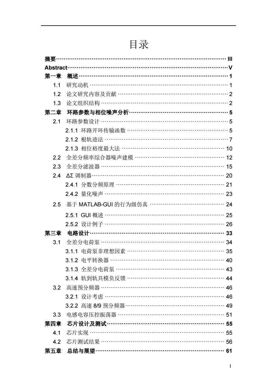
目录 摘要 …l川 Abstract-.............. …V 第一章概述… …1 1.1研究动机… …1 1.2论文研究内容及贡献… 2 1.3论文组织结构… …2 第二章环路参数与相位噪声分析 …5 2.1环路参数设计… …5 2.1.1环路开环传输函数 5 2.1.2根轨迹法 …7 2.1.3相位裕度最大法 10 2.2全差分频率综合器噪声建模 12 2.3全差分滤波器… 15 2.4△∑调制器… 20 2.4.1分数分频原理… 21 2.4.2量化噪声 23 2.5基于ATLAB-GUI的行为级仿真… 24 2.5.1GU概述 25 2.5.2设计例子… 26 第三章电路设计… 33 3.1全差分电荷泵… 34 3.1.1电荷泵非理想因素 35 3.1.2电平转换器… 40 3.1.3全差分电荷泵… 43 3.1.4轨到轨共模负反馈 44 3.2高速预分频器… 46 3.2.1设计考虑… 46 3.2.2高速8/9预分频器… 49 3.3电感电容压控振荡器 51 第四章芯片设计及测试… 55 4.1芯片实现 55 4.2芯片测试结果… 56 第五章总结与展望… 61
I 目录 摘要 ··························································································· III Abstract ······················································································ V 第一章 概述 ················································································ 1 1.1 研究动机 ·········································································· 1 1.2 论文研究内容及贡献 ··························································· 2 1.3 论文组织结构 ···································································· 2 第二章 环路参数与相位噪声分析 ····················································· 5 2.1 环路参数设计 ···································································· 5 2.1.1 环路开环传输函数 ······················································ 5 2.1.2 根轨迹法 ·································································· 7 2.1.3 相位裕度最大法 ······················································· 10 2.2 全差分频率综合器噪声建模 ················································ 12 2.3 全差分滤波器 ·································································· 15 2.4 ∆Σ 调制器······································································· 20 2.4.1 分数分频原理 ·························································· 21 2.4.2 量化噪声 ································································ 23 2.5 基于 MATLAB-GUI 的行为级仿真 ········································ 24 2.5.1 GUI 概述 ································································ 25 2.5.2 设计例子 ································································ 26 第三章 电路设计 ········································································ 33 3.1 全差分电荷泵 ·································································· 34 3.1.1 电荷泵非理想因素 ···················································· 35 3.1.2 电平转换器 ····························································· 40 3.1.3 全差分电荷泵 ·························································· 43 3.1.4 轨到轨共模负反馈 ···················································· 44 3.2 高速预分频器 ·································································· 46 3.2.1 设计考虑 ································································ 46 3.2.2 高速 8/9 预分频器 ····················································· 49 3.3 电感电容压控振荡器 ························································· 51 第四章 芯片设计及测试 ······························································· 55 4.1 芯片实现 ········································································ 55 4.2 芯片测试结果 ·································································· 56 第五章 总结与展望 ····································································· 61

5.1成果总结 61 5.2未来展望 62 致谢… 63
II 5.1 成果总结 ········································································ 61 5.2 未来展望 ········································································ 62 致谢 ·························································································· 63

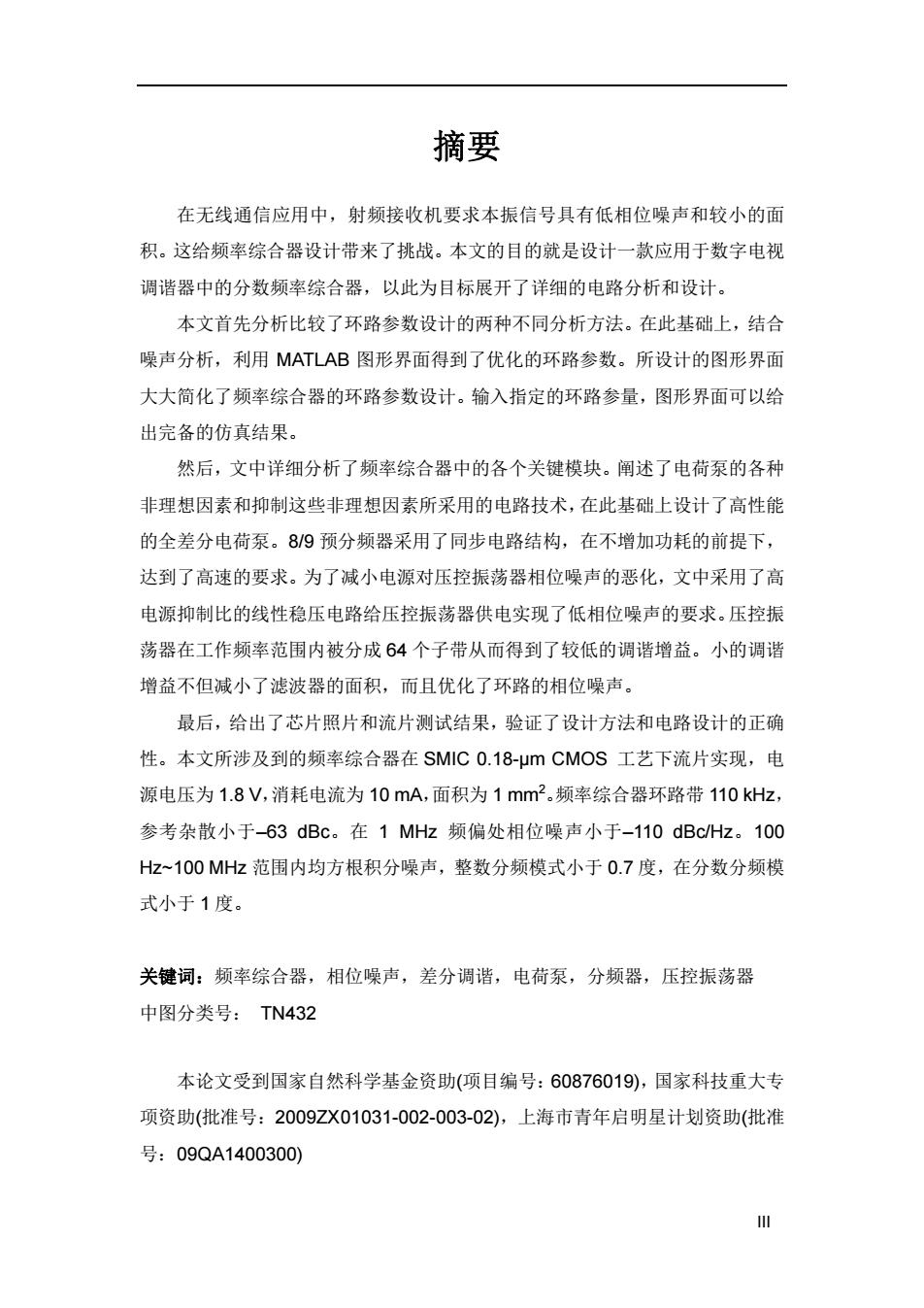
摘要 在无线通信应用中,射频接收机要求本振信号具有低相位噪声和较小的面 积。这给频率综合器设计带来了挑战。本文的目的就是设计一款应用于数字电视 调谐器中的分数频率综合器,以此为目标展开了详细的电路分析和设计。 本文首先分析比较了环路参数设计的两种不同分析方法。在此基础上,结合 噪声分析,利用MATLAB图形界面得到了优化的环路参数。所设计的图形界面 大大简化了频率综合器的环路参数设计。输入指定的环路参量,图形界面可以给 出完备的仿真结果。 然后,文中详细分析了频率综合器中的各个关键模块。阐述了电荷泵的各种 非理想因素和抑制这些非理想因素所采用的电路技术,在此基础上设计了高性能 的全差分电荷泵。8/9预分频器采用了同步电路结构,在不增加功耗的前提下, 达到了高速的要求。为了减小电源对压控振荡器相位噪声的恶化,文中采用了高 电源抑制比的线性稳压电路给压控振荡器供电实现了低相位噪声的要求。压控振 荡器在工作频率范围内被分成64个子带从而得到了较低的调谐增益。小的调谐 增益不但减小了滤波器的面积,而且优化了环路的相位噪声。 最后,给出了芯片照片和流片测试结果,验证了设计方法和电路设计的正确 性。本文所涉及到的频率综合器在SMIC0.18-μn CMOS工艺下流片实现,电 源电压为1.8V,消耗电流为10mA,面积为1mm2。频率综合器环路带110kHz, 参考杂散小于63dBc。在1MHz频偏处相位噪声小于-110dBc/Hz。100 Hz~100MHz范围内均方根积分噪声,整数分频模式小于0.7度,在分数分频模 式小于1度。 关键词:频率综合器,相位噪声,差分调谐,电荷泵,分频器,压控振荡器 中图分类号:TN432 本论文受到国家自然科学基金资助(项目编号:60876019),国家科技重大专 项资助(批准号:2009ZX01031-002-003-02),上海市青年启明星计划资助(批准 号:09QA1400300) 川
III 摘要 在无线通信应用中,射频接收机要求本振信号具有低相位噪声和较小的面 积。这给频率综合器设计带来了挑战。本文的目的就是设计一款应用于数字电视 调谐器中的分数频率综合器,以此为目标展开了详细的电路分析和设计。 本文首先分析比较了环路参数设计的两种不同分析方法。在此基础上,结合 噪声分析,利用 MATLAB 图形界面得到了优化的环路参数。所设计的图形界面 大大简化了频率综合器的环路参数设计。输入指定的环路参量,图形界面可以给 出完备的仿真结果。 然后,文中详细分析了频率综合器中的各个关键模块。阐述了电荷泵的各种 非理想因素和抑制这些非理想因素所采用的电路技术,在此基础上设计了高性能 的全差分电荷泵。8/9 预分频器采用了同步电路结构,在不增加功耗的前提下, 达到了高速的要求。为了减小电源对压控振荡器相位噪声的恶化,文中采用了高 电源抑制比的线性稳压电路给压控振荡器供电实现了低相位噪声的要求。压控振 荡器在工作频率范围内被分成 64 个子带从而得到了较低的调谐增益。小的调谐 增益不但减小了滤波器的面积,而且优化了环路的相位噪声。 最后,给出了芯片照片和流片测试结果,验证了设计方法和电路设计的正确 性。本文所涉及到的频率综合器在 SMIC 0.18-μm CMOS 工艺下流片实现,电 源电压为 1.8 V,消耗电流为 10 mA,面积为 1 mm2 。频率综合器环路带 110 kHz, 参考杂散小于–63 dBc。在 1 MHz 频偏处相位噪声小于–110 dBc/Hz。100 Hz~100 MHz 范围内均方根积分噪声,整数分频模式小于 0.7 度,在分数分频模 式小于 1 度。 关键词:频率综合器,相位噪声,差分调谐,电荷泵,分频器,压控振荡器 中图分类号: TN432 本论文受到国家自然科学基金资助(项目编号:60876019),国家科技重大专 项资助(批准号:2009ZX01031-002-003-02),上海市青年启明星计划资助(批准 号:09QA1400300)

Abstract RF receivers for wireless communication applications require LO with low phase noise and small area.These requirements present challenges for frequency synthesizer design.The main purpose of this paper is to design a fractional-N frequency synthesizer for DTV-tuner applications and based on the purpose much detailed circuits analysis and design is carried out. Firstly,two different loop parameters design methods are compared.Loop phase noise characteristic are analyzed and MATLAB GUI is developed to get proper loop parameters.The MATLAB GUI significantly simplifies the loop parameter design process.For given loop parameters,complete simulation results can be obtained. Secondly,several key modules in frequency synthesizers are presented. Different non-ideal factors in charge pump design are considered and circuit tricks to suppress these factors are combined in the presented fully-differential charge pump.The synchronized 8/9 prescaler is adopted achieving the speed requirements without extra power consumption.In order to minimize the VCO phase noise degradation from power supply,a high PSR LDO is employed. The VCO is split into 64 sub-bands to obtain a small tune gain to ensure a small area of LPF and at the same time the loop phase noise can be optimized. Thirdly,the chip photograph and test results are presented which demonstrates the analysis method and circuits design.The implemented frequency synthesizer draws 10 mA from a 1.8 V supply while occupying about 1 mm2 die area in SMIC 0.18-um CMOS process.The open loop bandwidth is 110 kHz and reference spur is less than-63 dBc.At 1 MHz frequency offset, the phase noise is less than-110 dBc/Hz.The RMS phase error integrated from 100 Hz to 100 MHz is less than 0.7 in integer-N mode and less than 1 in fractional-N mode. Key words:Frequency Synthesizer;Phase Noise;Differentially Tune;Charge Pump;Prescaler;Voltage-Controlled-Oscillator 小
V Abstract RF receivers for wireless communication applications require LO with low phase noise and small area. These requirements present challenges for frequency synthesizer design. The main purpose of this paper is to design a fractional-N frequency synthesizer for DTV-tuner applications and based on the purpose much detailed circuits analysis and design is carried out. Firstly, two different loop parameters design methods are compared. Loop phase noise characteristic are analyzed and MATLAB GUI is developed to get proper loop parameters. The MATLAB GUI significantly simplifies the loop parameter design process. For given loop parameters, complete simulation results can be obtained. Secondly, several key modules in frequency synthesizers are presented. Different non-ideal factors in charge pump design are considered and circuit tricks to suppress these factors are combined in the presented fully-differential charge pump. The synchronized 8/9 prescaler is adopted achieving the speed requirements without extra power consumption. In order to minimize the VCO phase noise degradation from power supply, a high PSR LDO is employed. The VCO is split into 64 sub-bands to obtain a small tune gain to ensure a small area of LPF and at the same time the loop phase noise can be optimized. Thirdly, the chip photograph and test results are presented which demonstrates the analysis method and circuits design. The implemented frequency synthesizer draws 10 mA from a 1.8 V supply while occupying about 1 mm2 die area in SMIC 0.18-µm CMOS process. The open loop bandwidth is 110 kHz and reference spur is less than –63 dBc. At 1 MHz frequency offset, the phase noise is less than –110 dBc/Hz. The RMS phase error integrated from 100 Hz to 100 MHz is less than 0.7° in integer-N mode and less than 1° in fractional-N mode. Key words:Frequency Synthesizer; Phase Noise; Differentially Tune; Charge Pump; Prescaler; Voltage-Controlled-Oscillator