
图4-22二分法直流失调矫正: 63 图4-23输入参考功率分布…64 图4-24PWD时间响应曲线… 64
V 图 4-22 二分法直流失调矫正·························································· 63 图 4-23 输入参考功率分布····························································· 64 图 4-24 PWD 时间响应曲线··························································· 64
表目录 表3-1放大器幅频响应和输出失调特性…24 表3-2过驱动电压…36 表3-3参考功率工艺角仿真结果…43 表3-4RSSl性能仿真结果…44 表4-1最高增益典型工艺角仿真结果…47 表4-2△V工艺角仿真结果…55 表4-3参考功率工艺角仿真结果…63 表4-4PWD性能总结…65 M
VI 表目录 表 3-1 放大器幅频响应和输出失调特性 ············································ 24 表 3-2 过驱动电压 ······································································· 36 表 3-3 参考功率工艺角仿真结果 ····················································· 43 表 3-4 RSSI 性能仿真结果 ···························································· 44 表 4-1 最高增益典型工艺角仿真结果 ··············································· 47 表 4-2 V 工艺角仿真结果···························································· 55 表 4-3 参考功率工艺角仿真结果 ····················································· 63 表 4-4 PWD 性能总结 ·································································· 65
摘要 现代数字电视调谐器广泛集成自动增益控制模块以扩大调谐器接受信号动 态范围。数字自动增益控制由于不会引入额外噪声,控制算法灵活等优点得到越 来越广泛的研究和应用。 本文主要工作是针对零中频数字调谐器中数字自动增益控制应用要求,设计 了一种低频接受信号强度指示电路和一款射频功率检测电路。 首先,简要介绍了调谐器自动增益控制的基础知识,包括干扰分析和接管点 等,并概述零中频接收机中一种数字自动增益控制方案。同时结合自动增益控制 的应用背景给出功率检测电路的性能参数。 其次,设计了一种低频接受信号强度指示电路。主要回顾连续检测结构的工 作原理,分析电路中放大器和整流器的输出误差,根据理论分析结果设计补偿电 路,并对器件失配做出优化。本次设计得到斜率为38.8 mv/dbm的功率检查曲线, 建立时间小于130us,检测范围为-20dBm~3dBm,频率范围为1KHz~20MHz, 功耗为2mw。 最后,设计一款射频功率检测电路。论文应用了一种单端数字功率检测结构, 主要分析探讨了电路的工作原理,频率特性,检测误差等方面,并且采用二分法 矫正输出直流失调。本次设计结果:频率范围为50M~860M,100us建立时间, 检测范围为-26dBm~-14dBM,功耗3.8mw。 本文所涉及功率检测电路均在TSMC0.18工艺下完成仿真设计。 关键词:数字电视调谐器、数字自动增益控制、接受信号强度指示器、射频功率 检测器、工艺温度补偿、直流失调矫正 中图分类号:TN432 1
1 摘 要 现代数字电视调谐器广泛集成自动增益控制模块以扩大调谐器接受信号动 态范围。数字自动增益控制由于不会引入额外噪声,控制算法灵活等优点得到越 来越广泛的研究和应用。 本文主要工作是针对零中频数字调谐器中数字自动增益控制应用要求,设计 了一种低频接受信号强度指示电路和一款射频功率检测电路。 首先,简要介绍了调谐器自动增益控制的基础知识,包括干扰分析和接管点 等,并概述零中频接收机中一种数字自动增益控制方案。同时结合自动增益控制 的应用背景给出功率检测电路的性能参数。 其次,设计了一种低频接受信号强度指示电路。主要回顾连续检测结构的工 作原理,分析电路中放大器和整流器的输出误差,根据理论分析结果设计补偿电 路,并对器件失配做出优化。本次设计得到斜率为38.8mv/dbm的功率检查曲线, 建立时间小于130us,检测范围为–20dBm~3dBm,频率范围为1KHz~20MHz, 功耗为2mw。 最后,设计一款射频功率检测电路。论文应用了一种单端数字功率检测结构, 主要分析探讨了电路的工作原理,频率特性,检测误差等方面,并且采用二分法 矫正输出直流失调。本次设计结果:频率范围为50M~860M,100us建立时间, 检测范围为–26dBm~–14dBM,功耗3.8mw。 本文所涉及功率检测电路均在TSMC0.18工艺下完成仿真设计。 关键词:数字电视调谐器、数字自动增益控制、接受信号强度指示器、射频功率 检测器、工艺温度补偿、直流失调矫正 中图分类号:TN432
Abstract In order to expand received signal dynamic range,automatic gain control modules are widely integrated in modern digital TV tuners.Because of the advantages of not introducing additional noise and flexible control algorithm, the programmable automatic gain control(PGC)is getting more and more research and application. This mainly work of this dissertation is design a low frequency received signal strength indicator(RSSI)and a radio frequency power detector(PWD), applying to PGC in the tuner with zero IF architecture. First,the basic knowledge of PGC is introduced briefly,including analysis of interference and take-over points,etc,an overview of a PGC scheme applying to zero IF receiver is also introduced.The circuit performance parameters of RSSI and PWD are given in terms of PGC application. Second,the design of RSSI is presented.The principle of successive detection architecture is reviewed;output errors of the amplifier and rectifier are discussed in detail.According to the theoretical analysis,compensation circuits are designed and the performance of device match is also optimized. In this design,the slop of RSSI is 38.8mv/dbm with150us settle time,detection range is-20dbm~3dbm,the effective frequency range can reach 20MHz,the power is 2mw. Finally,the design power detector circuit is introduced.A single ended digital control power detection structure is used.The principle of this architecture,frequency characteristics and detection error is analyzed.The bisection technique is used to calibrate output DC offset.In this work,the frequency band is 50M~860M with-26dBm~-14dBm detection range,the settle time is 100us,the total power is 3.8mw. All the circuits in this work are designed under TSMC0.18 process. Keywords:Digital TV tuner,PGC,RSSI,Power detector,corner and temperature Compensation,DC offset calibration Classification Code:TN432 3
3 Abstract In order to expand received signal dynamic range, automatic gain control modules are widely integrated in modern digital TV tuners. Because of the advantages of not introducing additional noise and flexible control algorithm, the programmable automatic gain control (PGC) is getting more and more research and application. This mainly work of this dissertation is design a low frequency received signal strength indicator (RSSI) and a radio frequency power detector (PWD), applying to PGC in the tuner with zero IF architecture. First, the basic knowledge of PGC is introduced briefly, including analysis of interference and take-over points, etc, an overview of a PGC scheme applying to zero IF receiver is also introduced. The circuit performance parameters of RSSI and PWD are given in terms of PGC application. Second, the design of RSSI is presented. The principle of successive detection architecture is reviewed; output errors of the amplifier and rectifier are discussed in detail. According to the theoretical analysis, compensation circuits are designed and the performance of device match is also optimized. In this design, the slop of RSSI is 38.8mv/dbm with150us settle time, detection range is –20dbm~3dbm, the effective frequency range can reach 20MHz, the power is 2mw. Finally, the design power detector circuit is introduced. A single ended digital control power detection structure is used. The principle of this architecture, frequency characteristics and detection error is analyzed. The bisection technique is used to calibrate output DC offset. In this work, the frequency band is 50M~860M with –26dBm~–14dBm detection range, the settle time is 100us, the total power is 3.8mw. All the circuits in this work are designed under TSMC0.18 process. Keywords: Digital TV tuner, PGC,RSSI,Power detector,corner and temperature Compensation,DC offset calibration Classification Code: TN432
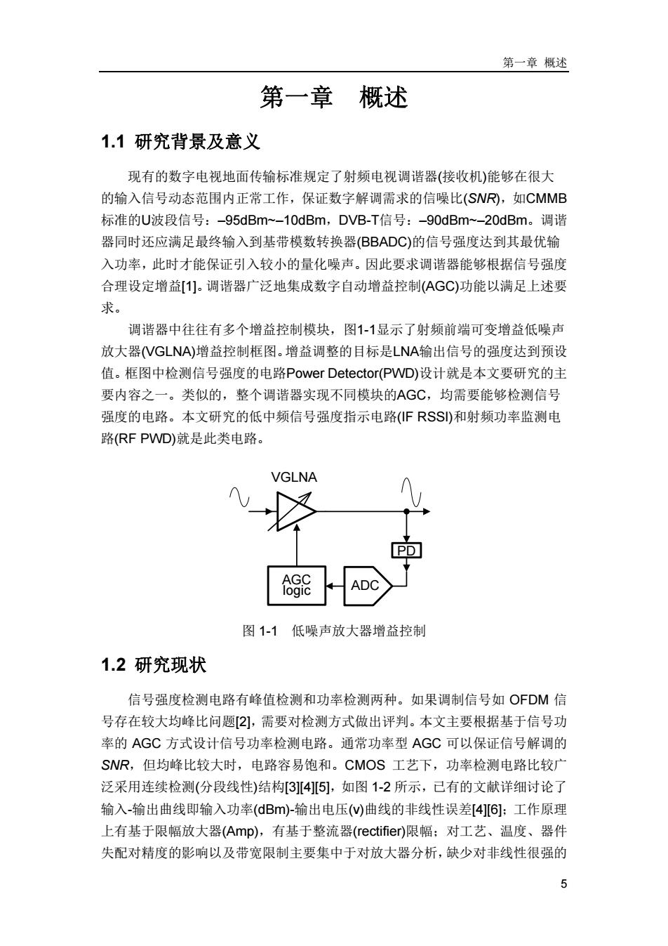
第一章概述 第一章概述 1.1研究背景及意义 现有的数字电视地面传输标准规定了射频电视调谐器(接收机)能够在很大 的输入信号动态范围内正常工作,保证数字解调需求的信噪比(SNR,如CMMB 标准的U波段信号:-95dBm~-10dBm,DVB-T信号:-90dBm~-20dBm。调谐 器同时还应满足最终输入到基带模数转换器(BBADC)的信号强度达到其最优输 入功率,此时才能保证引入较小的量化噪声。因此要求调谐器能够根据信号强度 合理设定增益[1]。调谐器广泛地集成数字自动增益控制(AGC)功能以满足上述要 求。 调谐器中往往有多个增益控制模块,图1-1显示了射频前端可变增益低噪声 放大器VGLNA)增益控制框图。增益调整的目标是LNA输出信号的强度达到预设 值。框图中检测信号强度的电路Power Detector(PWD)设计就是本文要研究的主 要内容之一。类似的,整个调谐器实现不同模块的AGC,均需要能够检测信号 强度的电路。本文研究的低中频信号强度指示电路(FRSS)和射频功率监测电 路(RF PWD)就是此类电路。 VGLNA AGC logic 图1-1低噪声放大器增益控制 1.2研究现状 信号强度检测电路有峰值检测和功率检测两种。如果调制信号如OFDM信 号存在较大均峰比问题2],需要对检测方式做出评判。本文主要根据基于信号功 率的AGC方式设计信号功率检测电路。通常功率型AGC可以保证信号解调的 SWR,但均峰比较大时,电路容易饱和。CMOS工艺下,功率检测电路比较广 泛采用连续检测(分段线性)结构[3][4[5],如图1-2所示,己有的文献详细讨论了 输入-输出曲线即输入功率(dBm)-输出电压()曲线的非线性误差[4][6]:工作原理 上有基于限幅放大器(Amp),有基于整流器(rectifier)限幅;对工艺、温度、器件 失配对精度的影响以及带宽限制主要集中于对放大器分析,缺少对非线性很强的 5
第一章 概述 5 第一章 概述 1.1 研究背景及意义 现有的数字电视地面传输标准规定了射频电视调谐器(接收机)能够在很大 的输入信号动态范围内正常工作,保证数字解调需求的信噪比(SNR),如CMMB 标准的U波段信号:–95dBm~–10dBm,DVB-T信号:–90dBm~–20dBm。调谐 器同时还应满足最终输入到基带模数转换器(BBADC)的信号强度达到其最优输 入功率,此时才能保证引入较小的量化噪声。因此要求调谐器能够根据信号强度 合理设定增益[1]。调谐器广泛地集成数字自动增益控制(AGC)功能以满足上述要 求。 调谐器中往往有多个增益控制模块,图1-1显示了射频前端可变增益低噪声 放大器(VGLNA)增益控制框图。增益调整的目标是LNA输出信号的强度达到预设 值。框图中检测信号强度的电路Power Detector(PWD)设计就是本文要研究的主 要内容之一。类似的,整个调谐器实现不同模块的AGC,均需要能够检测信号 强度的电路。本文研究的低中频信号强度指示电路(IF RSSI)和射频功率监测电 路(RF PWD)就是此类电路。 VGLNA PD ADC AGC logic 图 1-1 低噪声放大器增益控制 1.2 研究现状 信号强度检测电路有峰值检测和功率检测两种。如果调制信号如 OFDM 信 号存在较大均峰比问题[2],需要对检测方式做出评判。本文主要根据基于信号功 率的 AGC 方式设计信号功率检测电路。通常功率型 AGC 可以保证信号解调的 SNR,但均峰比较大时,电路容易饱和。CMOS 工艺下,功率检测电路比较广 泛采用连续检测(分段线性)结构[3][4][5],如图 1-2 所示,已有的文献详细讨论了 输入-输出曲线即输入功率(dBm)-输出电压(v)曲线的非线性误差[4][6];工作原理 上有基于限幅放大器(Amp),有基于整流器(rectifier)限幅;对工艺、温度、器件 失配对精度的影响以及带宽限制主要集中于对放大器分析,缺少对非线性很强的