IMAGE SENSORS DATA SHEET hiiic FT18 1M Frame Transfer CCD Image Sensor Product specification 2006 December 19 DALSA Professional Imaging DALSA
IMAGE SENSORS DATA SHEET FT18 1M Frame Transfer CCD Image Sensor Product specification 2006 December 19 DALSA Professional Imaging

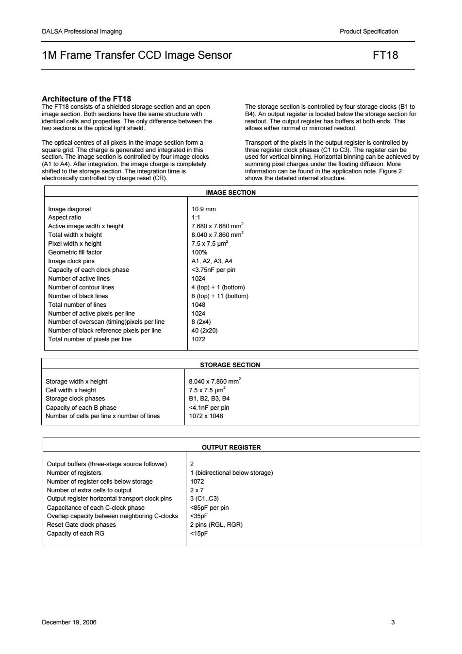
DALSA Professional maging Product Specification 1M Frame Transfer CCD Image Sensor FT18 2/3-inch optical format 1M active pixels(1024H x 1024V) Progressive scan Excellont antiblooming Variable electronic shuttering Square pixel structure H and V binning 100%optical fill factor High dynamic range (>60dB) VV120 High sensitivity Low dark current and fixed pattern noise Low readout noise Data rate up to 40 MHz Description Frame rate up to 30 Hz The monc Mirrored readout option gh a RoHS compliant (Pb 1 blac Device structure 4. m 17omm 1024 active pixe 1072 1024( secon 1072 cells Output register Figure1-Device structure December19.200
DALSA Professional Imaging Product Specification 1M Frame Transfer CCD Image Sensor FT18 December 19, 2006 2 • 2/3-inch optical format • 1M active pixels (1024H x 1024V) • Progressive scan • Excellent antiblooming • Variable electronic shuttering • Square pixel structure • H and V binning • 100% optical fill factor • High dynamic range (>60dB) • High sensitivity • Low dark current and fixed pattern noise • Low readout noise • Data rate up to 40 MHz • Frame rate up to 30 Hz • Mirrored readout option • RoHS compliant Description The FT18 is a monochrome progressive-scan frame transfer image sensor offering 1K x 1K pixels at 30 frames per second through a single output buffer. The combination of high speed and a high linear dynamic range (>10 true bits at room temperature without cooling) makes this device the perfect solution for high-end real time medical x-ray, scientific, and industrial applications. A second output can be used for mirrored images. The device structure is shown in Figure 1. Device structure Figure 1 - Device structure 1024 active pixels 1 contour line 8 black lines 20 4 Optical size: 7.68 mm (H) x 7.68 mm (V) Chip size: 8.9 mm (H) x 17.0 mm (V) Pixel size: 7.5 µm x 7.5 µm Active pixels: 1024 (H) x 1024 (V) Total no. of pixels: 1072 (H) x 1048 (V) Optical black pixels: Left: 20 Right:20 Timing pixels: Left: 4 Right:4 Dummy register pixels: Left: 7 Right: 7 Contour lines: Bottom: 1 Top: 4 Optical black lines: Bottom: 11 Top: 8 20 Image Section Storage Section Output amplifier 1072 cells Output register 7 7 2096 lines 1024 active lines 4 8 black lines 11 black lines 4 contour lines
Product Specfication 1M Frame Transfer CCD Image Sensor FT18 sectior n the for ve ved by (A1 t0A4)Ae in e nder the fl IMAGE SECTION 007e0m ge clock pins A1.A2.A3.M4 ock phase Number of activeines 1024 SnF per pir of lines 02 lumber of 824 1072 STORAGE SECTION orage clock ph Number of cls per 1072x1046 OUTPUT REGISTER stage source follower) storage tou t register h ntal tr t clock pins 3(C1C3) ap capacity be ighboring C-clocks acity of each RG 215pF (RGL.RGR) December19.00
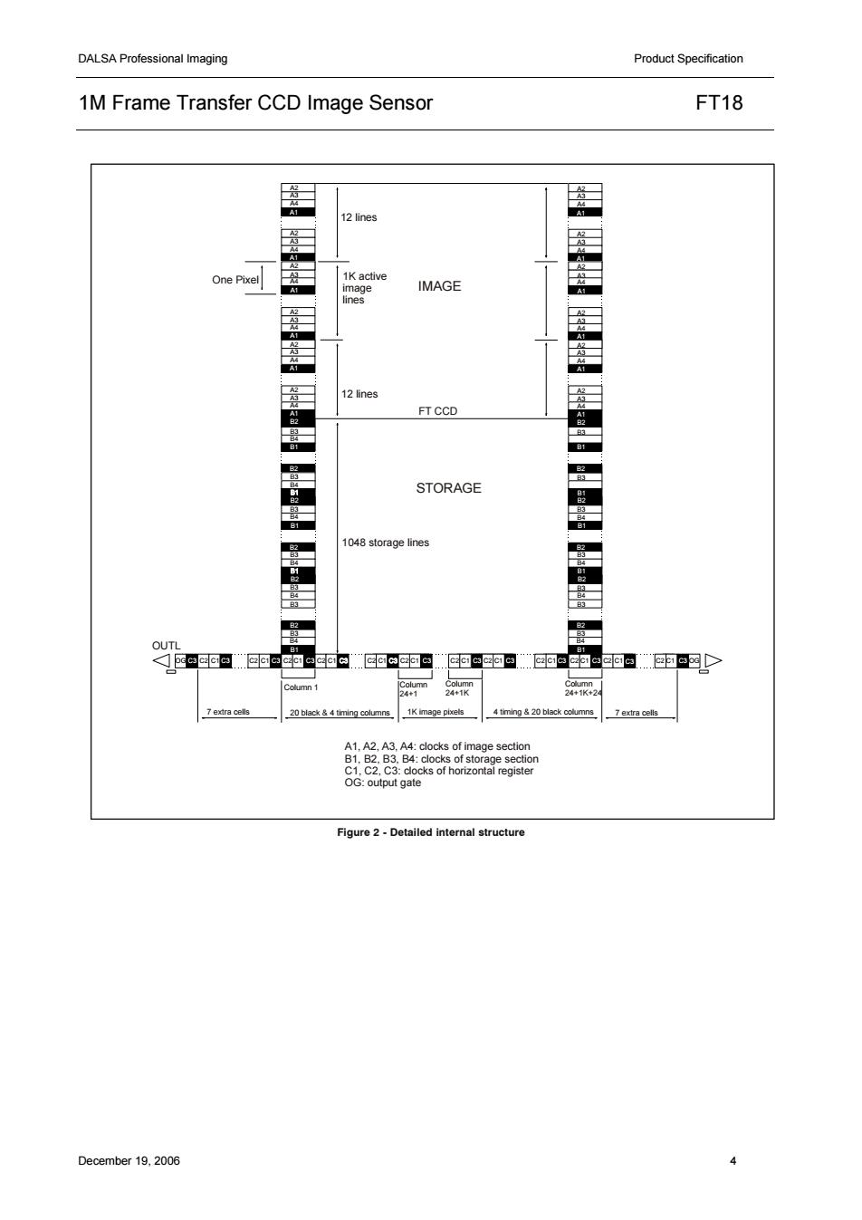
DALSA Professional Imaging Product Specification 1M Frame Transfer CCD Image Sensor FT18 December 19, 2006 3 Architecture of the FT18 The FT18 consists of a shielded storage section and an open image section. Both sections have the same structure with identical cells and properties. The only difference between the two sections is the optical light shield. The optical centres of all pixels in the image section form a square grid. The charge is generated and integrated in this section. The image section is controlled by four image clocks (A1 to A4). After integration, the image charge is completely shifted to the storage section. The integration time is electronically controlled by charge reset (CR). The storage section is controlled by four storage clocks (B1 to B4). An output register is located below the storage section for readout. The output register has buffers at both ends. This allows either normal or mirrored readout. Transport of the pixels in the output register is controlled by three register clock phases (C1 to C3). The register can be used for vertical binning. Horizontal binning can be achieved by summing pixel charges under the floating diffusion. More information can be found in the application note. Figure 2 shows the detailed internal structure. IMAGE SECTION Image diagonal Aspect ratio Active image width x height Total width x height Pixel width x height Geometric fill factor Image clock pins Capacity of each clock phase Number of active lines Number of contour lines Number of black lines Total number of lines Number of active pixels per line Number of overscan (timing)pixels per line Number of black reference pixels per line Total number of pixels per line 10.9 mm 1:1 7.680 x 7.680 mm2 8.040 x 7.860 mm2 7.5 x 7.5 µm2 100% A1, A2, A3, A4 <3.75nF per pin 1024 4 (top) + 1 (bottom) 8 (top) + 11 (bottom) 1048 1024 8 (2x4) 40 (2x20) 1072 OUTPUT REGISTER Output buffers (three-stage source follower) Number of registers Number of register cells below storage Number of extra cells to output Output register horizontal transport clock pins Capacitance of each C-clock phase Overlap capacity between neighboring C-clocks Reset Gate clock phases Capacity of each RG 2 1 (bidirectional below storage) 1072 2 x 7 3 (C1.C3) <85pF per pin <35pF 2 pins (RGL, RGR) <15pF STORAGE SECTION Storage width x height Cell width x height Storage clock phases Capacity of each B phase Number of cells per line x number of lines 8.040 x 7.860 mm2 7.5 x 7.5 µm2 B1, B2, B3, B4 <4.1nF per pin 1072 x 1048
DALSA Professional maging Product 1M Frame Transfer CCD Image Sensor FT18 12 nes 图 屋 IMAGE 居 FT CCD 图 STORAGE 思 国 1048soageine 3:doc December19.06 4
DALSA Professional Imaging Product Specification 1M Frame Transfer CCD Image Sensor FT18 December 19, 2006 4 Figure 2 - Detailed internal structure A1, A2, A3, A4: clocks of image section B1, B2, B3, B4: clocks of storage section C1, C2, C3: clocks of horizontal register OG: output gate STORAGE IMAGE FT CCD 12 lines 1K active image lines 12 lines One Pixel 1048 storage lines OUTL 7 extra cells 20 black & 4 timing columns 1K image pixels 4 timing & 20 black columns 7 extra cells Column 1 Column 24+1 Column 24+1K Column 24+1K+24 A2 A3 A4 A2 A3 A4 A2 A3 A4 A2 A3 A4 A2 A3 A4 A2 A3 A4 B3 B4 B3 B4 B3 B4 B3 B4 B3 B4 B3 B3 B4 A1 A1 A1 A1 A1 B2 B1 B2 B2 B1 B1 B2 B2 B2 B1 C3 C3 C3 C3 C3 C3 C3 C3 C3 C3 C3 A2 A3 A4 A2 A3 A4 A2 A3 A4 A2 A3 A4 A2 A3 A4 A2 A3 A4 B3 B3 B3 B4 B3 B4 B3 B4 B3 B3 B4 A1 A1 A1 A1 A1 B2 B1 B2 B2 B1 B1 B2 B1 B2 B2 B1 OG C2 C1 C2 C1 C2 C1 C2 C1 C2 C1 C2 C1 C2 C1 C2 C1 C2 C1 C2 C1 C2 C1 C2 C1 OG A1 A1
Product Specfication 1M Frame Transfer CCD Image Sensor FT18 JTE MAXIMUM RATINGS MIN MAX UNIT GENERAL: duringoperation oltage between any two aates +20 DC current through any clock(absolute value) 02 +02 OUT current (no short circuit protection) 0 +6 mA VOLTAGES IN RELATION TO VNS: SFD R -15 +05 All other pins 32 +0.5 VOLTAGES IN RELATION TO VPS: VNS SESO RD 50 All other pins -20 +20 DC CONDITIONS' MIN M TYPICAL [V MAX [V] UNIT VNS N substrate adjusted VPS well 18 0 >> OG Output Gate 5.4 8 RD Reset Drain 12 13 15 AC CLOCK LEVEL CONDITIONS' MIN TYPICAL MAX UNIT MAGE CLCKS (duty cyde-s8) A-clock low level 9.5 0 > Charge Reset (CR)level on A-clocks Charge Pump(CP)level onA-clocks 0 STORAGE CLOCKS(duty cycle 5/8) 95 10 C-clock swing 5 C-clock low level 3 OTHER CLOCKS: 10. December19.00 5
DALSA Professional Imaging Product Specification 1M Frame Transfer CCD Image Sensor FT18 December 19, 2006 5 Specifications ABSOLUTE MAXIMUM RATINGS MIN MAX UNIT GENERAL: storage temperature -55 +80 ºC ambient temperature during operation -40 +60 ºC voltage between any two gates -20 +20 V DC current through any clock (absolute value) -0.2 +0.2 µA OUT current (no short circuit protection) 0 +6 mA VOLTAGES IN RELATION TO VNS: VPS, SFS -30 +0.5 V SFD -8 +8 V RD -15 +0.5 V All other pins -32 +0.5 V VOLTAGES IN RELATION TO VPS: VNS -0.5 +30 V SFD, RD +0 +30 V SFS -8 +8 V All other pins -20 +20 V DC CONDITIONS1 MIN [V] TYPICAL [V] MAX [V] UNIT VNS2 N substrate 16 adjusted 24 V VPS P well 2 4 6 V SFD Source Follower Drain 18 20 22 V SFS Source Follower Source - 0 - V VCS Current Source Gate -2 0 3 V OG Output Gate 3 5.4 8 V RD Reset Drain 12 13 15 V AC CLOCK LEVEL CONDITIONS1 MIN TYPICAL MAX UNIT IMAGE CLOCKS (duty cycle = 5/8) A-clock swing 9.5 10 - V A-clock low level - 0 - V Charge Reset (CR) level on A-clocks3 - -5 - V Charge Pump (CP) level on A-clocks - 0 - V STORAGE CLOCKS (duty cycle = 5/8) B-clock swing 9.5 10 - V B-clock low level - 0 - V OUTPUT REGISTER CLOCKS (duty cycle = 1/2) C-clock swing - 5 - V C-clock low level - 3 - V OTHER CLOCKS: Reset Gate (RG) swing - 10 12 V Reset Gate (RG) low level - 1 - V 1 All voltages in relation to SFS. 2 To set the VNS voltage for optimal Vertical Antiblooming (VAB), it should be adjustable between minimum and maximum values. 3 Guaranteed charge requires the CR voltage to last at least 1.2µs