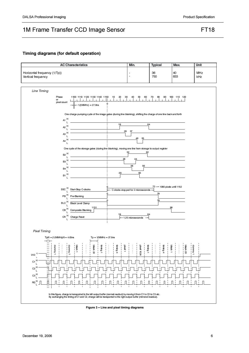
Product 1M Frame Transfer CCD Image Sensor FT18 Timing diagrams(for default operation) Min. Typical Max. Unit 0"02e129用399男mm92m00 、-1304t=27.88 B3 B H 20 SsC M surt-Sop C-dooks Piel Timing H- 几几 igur3-Line and pixel timing diagrams December19.0 6
DALSA Professional Imaging Product Specification 1M Frame Transfer CCD Image Sensor FT18 December 19, 2006 6 Timing diagrams (for default operation) Figure 3 – Line and pixel timing diagrams H L H L H L C1 C2 C3 Tp/6 = (1/36MHz)/6 = 4.63ns dum my 1 . . . . . . . dum my 7 black 1 . . . . . . . black 20 timing 1 timing 4 pixel 1 . . . . . . . pixel 1024 timing 1 timing 4 black 1 . . . . . . . black 20 dum my 1 H L RG Tp = 1/36MHz = 27.8ns . . . . . . . . . . . . . . In this figure, charge is transported to the left output buffer (normal readout) by moving it from C1 to C2 to C3 etc. By exchanging the timing of C1 and C2, charge will be transported to the right output buffer (mirrored readout). A1 A2 A3 A4 Phase or pixel count 1100 1110 1120 1130 1140 10 20 30 40 50 60 70 80 90 100 110 120 L H L H L H L H B2 B3 B4 B1 L H L H L H L H 19 64 28 37 46 55 32 62 26 44 38 56 20 50 SSC L H 72 1150 0 0 One cycle of the storage gates (during line blanking), moving one line from storage to output register C clocks stopped for 2 microseconds L H PB 0 L H BLC 0 79 79 L H CB 1131 99 1080 pixels until 1152 1/(36MHz) = 27.8ns One charge pumping cycle of the image gates (during line blanking), shifting the charge of one line back and forth Start-Stop C-clocks Pre-Blanking Black Level Clamp Composite Blanking L CR 19 64 Charge Reset H 1.25 microseconds AC Characteristics Min. Typical Max. Unit Horizontal frequency (1/Tp)) Vertical frequency - Line Timing Pixel Timing - 36 750 40 833 MHz kHz
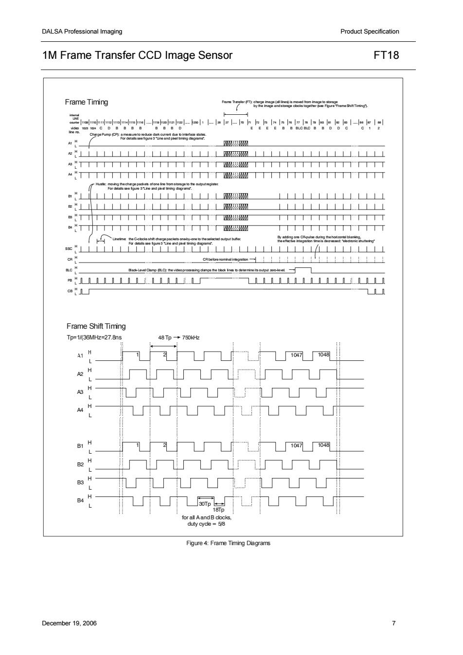
Product Specfication 1M Frame Transfer CCD Image Sensor FT18 Frame Timing o上ehs “L上山L盈题 ⊥L上上⊥L =“L⊥LLLL山L上上L上L上L孤题题 1111111111111 TIIITI盈 TIII “TT十十十TT十门T1T11717磁题 中 Frame Shift Timing p-136MHz=27,8 48Tp70 104710 A3 H 1047104 H B4 Figure 4:Frame Timing Dagrams December19.00
DALSA Professional Imaging Product Specification 1M Frame Transfer CCD Image Sensor FT18 December 19, 2006 7 A2 L H A3 L H A4 L H 1 2 1048 1047 B1 L H B2 L H B3 L H B4 L H 1 2 1048 1047 48 Tp 750kHz 18Tp 30Tp for all A and B clocks, duty cycle = 5/8 1109 1110 1111 1112 1113 1114 1115 1116 1119 1120 1121 1122 . 1250 1 . 26 27 . 70 71 72 73 74 75 76 77 78 79 80 81 82 83 86 87 1023 1024 CDBBB B B BB D internal LINE counter video E E E E B B BLC BLC B B D D C C 1 line no. A1 A2 A3 A4 L H L H L H L H B1 B2 B3 B4 L H L H L H L H CR BLC SSC PB L H L H L H L H By adding one CR-pulse during the horizontal blanking, the effective integration time is decreased: "electronic shuttering" CB L H CR before nominal integration . . 88 2 charge image (all lines) is moved from image to storage by the image and storage clocks together (see Figure "Frame Shift Timing"). Frame Transfer (FT): Charge Pump (CP): a measure to reduce dark current due to interface states. For details see figure 3 "Line and pixel timing diagrams". Hustle: moving the charge packets of one line from storage to the output register. For details see figure 3 "Line and pixel timing diagrams". Linetime: the C-clocks shift charge packets one-by-one to the selected output buffer. For details see figure 3 "Line and pixel timing diagrams". Black-Level Clamp (BLC): the video processing clamps the black lines to determine its output zero-level. Figure 4: Frame Timing Diagrams Frame Timing Frame Shift Timing Tp=1/(36MHz=27.8ns