二、集成电路中的电阻 无源(passive)电阻 通常是合金材料或采用掺杂半导体制作的电阻 ●有源(active)电阻 将晶体管进行适当的连接和偏置,利用晶体管 的不同的工作区所表现出来的不同的电阻特性来做 电阻
二、 集成电路中的电阻 l 无源(passive)电阻 通常是合金材料或采用掺杂半导体制作的电阻 l 有源(active)电阻 将晶体管进行适当的连接和偏置,利用晶体管 的不同的工作区所表现出来的不同的电阻特性来做 电阻
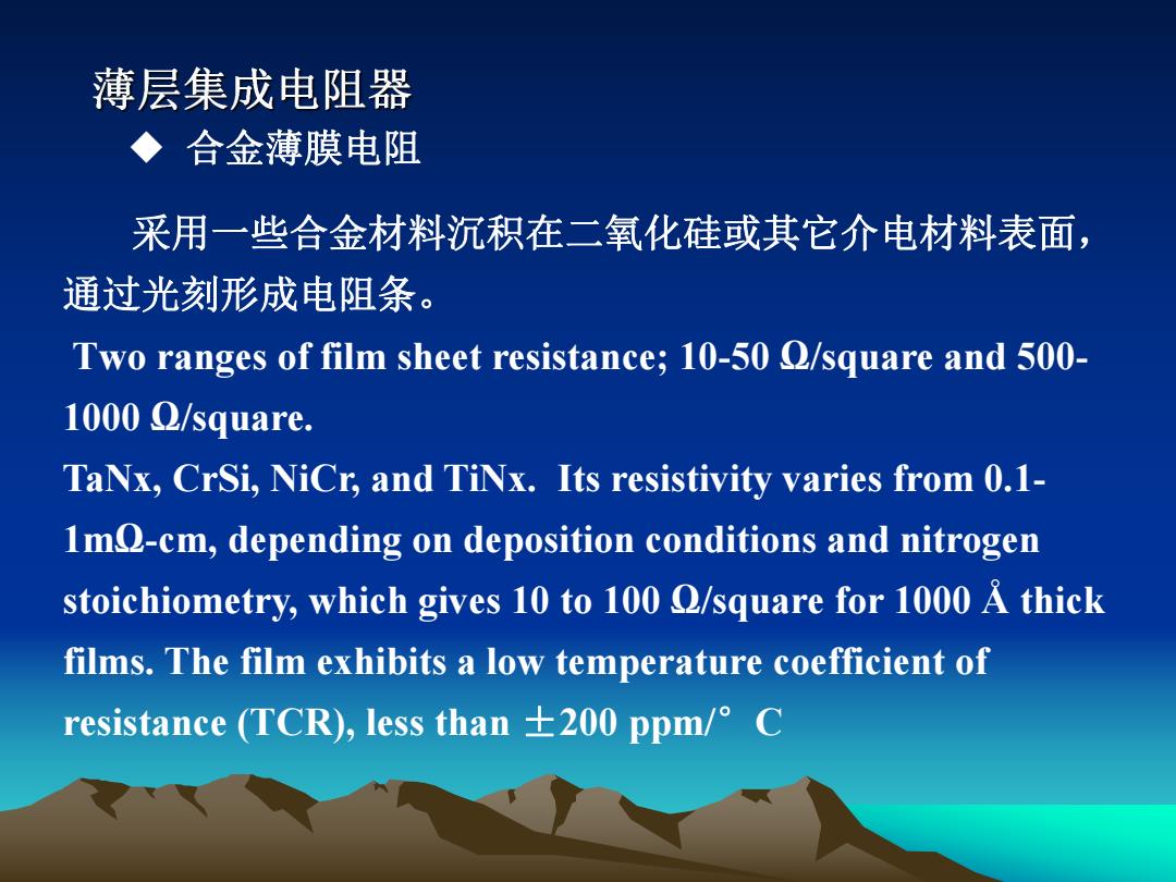
薄层集成电阻器 ◆合金薄膜电阻 采用一些合金材料沉积在二氧化硅或其它介电材料表面, 通过光刻形成电阻条。 Two ranges of film sheet resistance;10-50 Q/square and 500- 1000①/square. TaNx,CrSi,NiCr,and TiNx.Its resistivity varies from 0.1- 1mQ-cm,depending on deposition conditions and nitrogen stoichiometry,which gives 10 to 100 Q/square for 1000 A thick films.The film exhibits a low temperature coefficient of resistance(TCR),less than±200ppm/°C
u 合金薄膜电阻 采用一些合金材料沉积在二氧化硅或其它介电材料表面, 通过光刻形成电阻条。 Two ranges of film sheet resistance; 10-50 Ω/square and 500- 1000 Ω/square. TaNx, CrSi, NiCr, and TiNx. Its resistivity varies from 0.1- 1mΩ-cm, depending on deposition conditions and nitrogen stoichiometry, which gives 10 to 100 Ω/square for 1000 Å thick films. The film exhibits a low temperature coefficient of resistance (TCR), less than ±200 ppm/°C
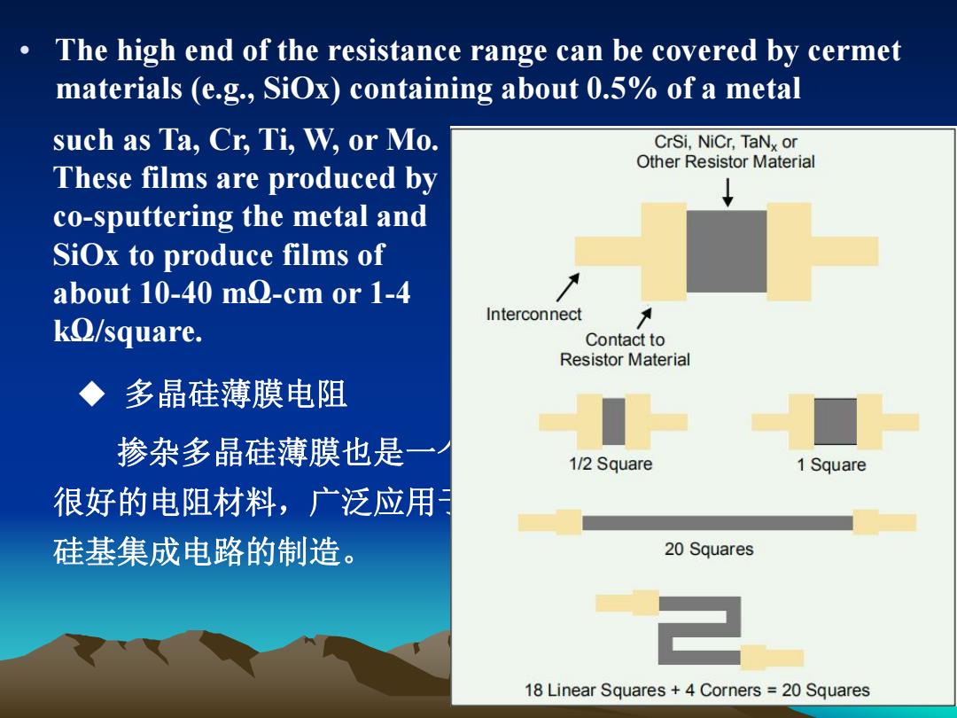
The high end of the resistance range can be covered by cermet materials (e.g.,SiOx)containing about 0.5%of a metal such as Ta,Cr,Ti,W,or Mo. CrSi,NiCr,TaNy or Other Resistor Material These films are produced by co-sputtering the metal and SiOx to produce films of about 10-40 mQ-cm or 1-4 Interconnect kQ/square. Contact to Resistor Material 多晶硅薄膜电阻 掺杂多晶硅薄膜也是 1/2 Square 1 Square 很好的电阻材料,广泛应用 硅基集成电路的制造。 20 Squares 18 Linear Squares +4 Corners 20 Squares
• The high end of the resistance range can be covered by cermet materials (e.g., SiOx) containing about 0.5% of a metal 掺杂多晶硅薄膜也是一个 很好的电阻材料,广泛应用于 硅基集成电路的制造。 u 多晶硅薄膜电阻 such as Ta, Cr, Ti, W, or Mo. These films are produced by co-sputtering the metal and SiOx to produce films of about 10-40 mΩ-cm or 1-4 kΩ/square
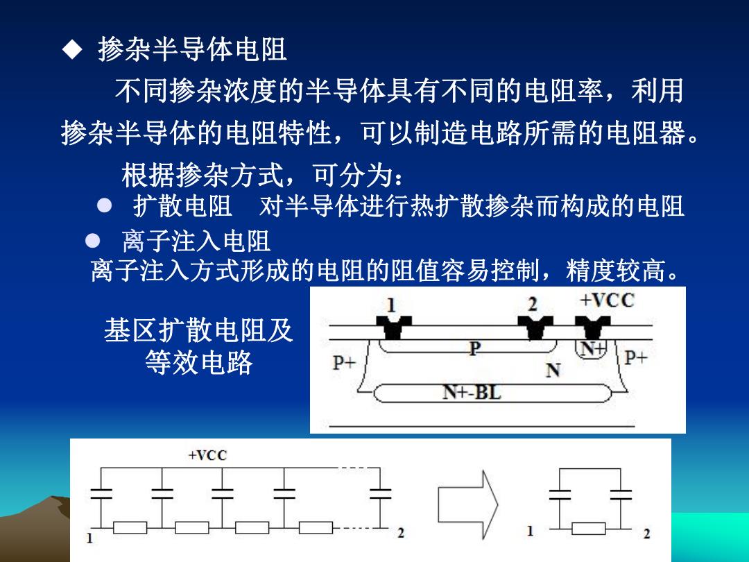
掺杂半导体电阻 不同掺杂浓度的半导体具有不同的电阻率,利用 掺杂半导体的电阻特性,可以制造电路所需的电阻器。 根据掺杂方式,可分为: 扩散电阻对半导体进行热扩散掺杂而构成的电阻 离子注入电阻 离子注入方式形成的电阻的阻值容易控制,精度较高。 +VCC 基区扩散电阻及 等效电路 N N+-BL +VCC 1
u 掺杂半导体电阻 不同掺杂浓度的半导体具有不同的电阻率,利用 掺杂半导体的电阻特性,可以制造电路所需的电阻器。 根据掺杂方式,可分为: l 离子注入电阻 l 扩散电阻 对半导体进行热扩散掺杂而构成的电阻 离子注入方式形成的电阻的阻值容易控制,精度较高。 基区扩散电阻及 等效电路
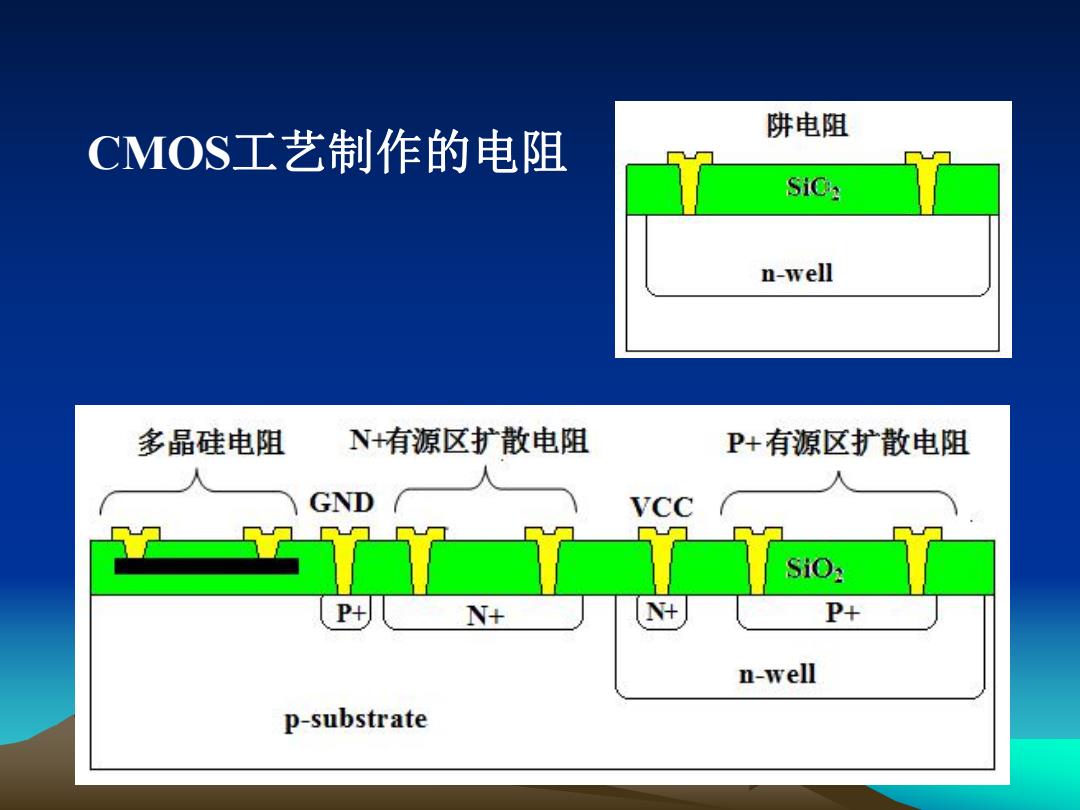
阱电阻 CMOS工艺制作的电阻 SiC: n-well 多晶硅电阻 N+有源区扩散电阻 P+有源区扩散电阻 GND VCC SiO: P+ N+ N+ P+ n-well p-substrate
CMOS工艺制作的电阻