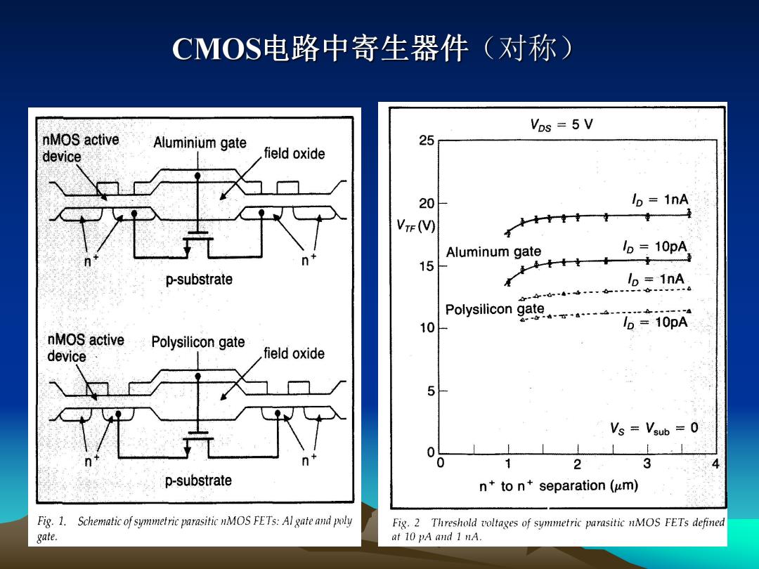
CMOS电路中寄生器件(对称) Vos =5V nMOS active Aluminium gate 25 device field oxide 20 lo 1nA VTF (V) Aluminum gate 15 p-substrate lp=1nA Polysilicon 10 lp=10pA nMOS active Polysilicon gate device field oxide 5 Vs Vsub=0 0 2 3 p-substrate n*to n+separation (um) Fig.1.Schematic of symmetric parasitic nMOS FETs:Al gate and poly Fig.2 Threshold voltages of symmetric parasitic nMOS FETs defined gate. at 10 pA and 1 nA

CMOS电路中寄生器件(非对称) measured values 16 i 20 Aluminum gate modeled values nMOS黄 12 -40 field oxide 8 -60 pMOS p-substrate n-well n+to n-well 80 MOSFET p+to p-substrate MOSFET Vs=VSUB=0 0 -100 Fig.3 Schematic of asymmetric parasitic MOSFETs with Al gate in a 2 3 CMOS structure. Nominal separation(um) Fig.6 Measured and simulated threshold voltages for the asymmetric parasitic FETs with Al gate;nominal separation represents n'-to-n-well or p-to-p-sub spacing for nMOS or pMOS FETs,respectively
CMOS电路中寄生器件(非对称)
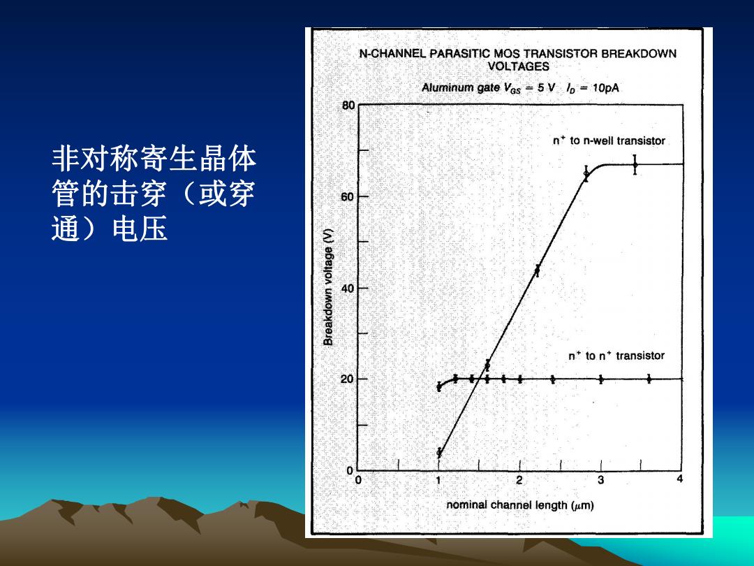
N-CHANNEL PARASITIC MOS TRANSISTOR BREAKDOWN VOLTAGES Aluminum gate Vas =5 V lo=10pA 80 n*to n-well transistor 非对称寄生晶体 管的击穿(或穿 60 通)电压 40 n'to n'transistor 20 2 3 nominal channel length (um)
非对称寄生晶体 管的击穿(或穿 通)电压
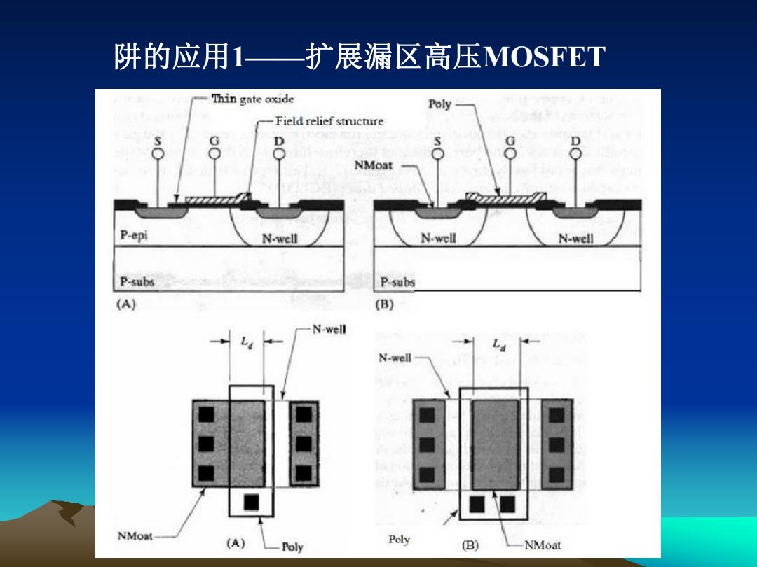
阱的应用1—扩展漏区高压MOSFET Thin gate oxide Poly Field relief structure G D G D NMoat P-epi N-well N-well N-well P-subs P-subs (A) (B) N-well N-well ■■ ■■ NMoat (A) Poly Poly (B) NMoat
阱的应用1——扩展漏区高压MOSFET
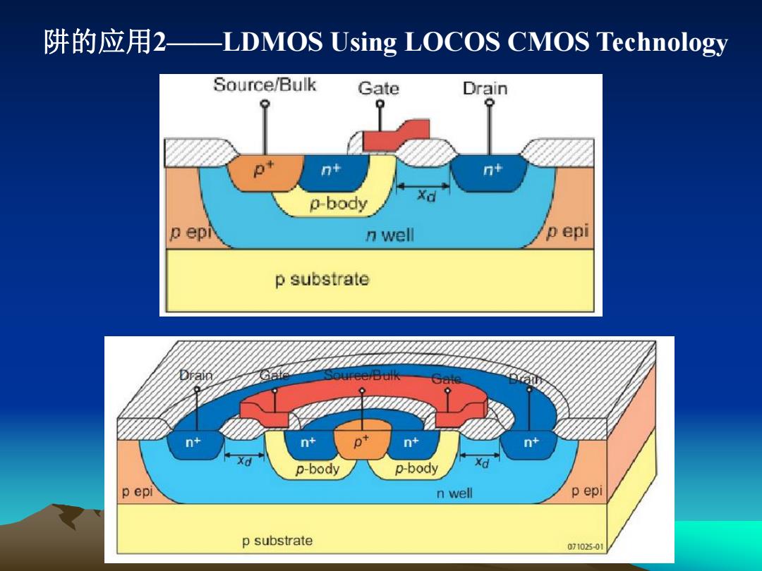
阱的应用2-LDMOS Using LOCOS CMOS Technology Source/Bulk Gate Drain n+ n+ o-body 产Xd p epr n well p epi p substrate uree/Bulk n+ p-body p-body Xd p epi n well p epi p substrate 071025-01
阱的应用2——LDMOS Using LOCOS CMOS Technology