
人工智能芯片发展历程 背景 GPU、CPU设计比对 CPU CPU需要很强通用性处理不同数据类型,同时需要逻辑判断,还会 引入大量分支跳转和中断处理。 ALU ALU GPU ●由专为串行处理而优化的几个核心组成 Control ALU ALU TPU ●基于低延时设计 Cache FPGA √强大的ALU单元,可在很短时钟周期完成计算 √大量缓存降低延时 DRAM SOC √高时钟频率 CPU √复杂逻辑控制单元,多分支程序可通过分支预测能力降低时延 ● 擅长逻辑控制、串行运算
人工智能芯片发展历程 GPU、CPU设计比对 CPU需要很强通用性处理不同数据类型,同时需要逻辑判断,还会 引入大量分支跳转和中断处理。 由专为串行处理而优化的几个核心组成 基于低延时设计 强大的ALU单元,可在很短时钟周期完成计算 大量缓存降低延时 高时钟频率 复杂逻辑控制单元,多分支程序可通过分支预测能力降低时延 擅长逻辑控制、串行运算 GPU 背景 CPU TPU FPGA SOC
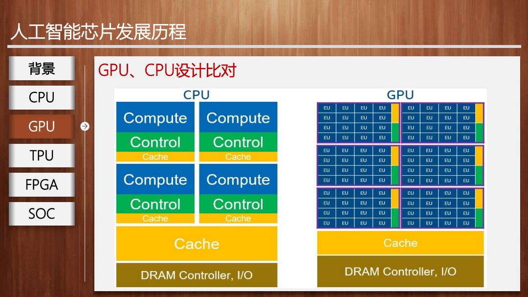
人工智能芯片发展历程 背景 GPU、CPU设计比对 CPU CPU GPU EU EU EU EU EU U EU EU GPU Compute Compute EU EU EU EU EU EU EU EU EU EU EU EU EU EU EU EU Control Control EU EU EU U U EU EU U TPU EU EU EU EU EU EU EU EU Cache Cache EU EU U EU EU EU EU EU EU EU EU EU EU EU EU EU FPGA Compute Compute EU EU EU EU EU EU EU EU EU EU EU EU EU EU EU Control Control EU EU EU EU EU EU EU EU SOC EU EU EU EU EU EU EU EU Cache Cache EU EU EU EU EU EU EU ② Cache Cache DRAM Controller,I/O DRAM Controller,I/O
人工智能芯片发展历程 GPU、CPU设计比对 GPU 背景 CPU TPU FPGA SOC
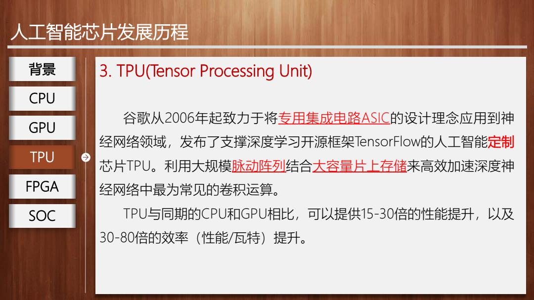
人工智能芯片发展历程 背景 3.TPU(Tensor Processing Unit) CPU 谷歌从2006年起致力于将专用集成电路ASIC的设计理念应用到神 GPU 经网络领域,发布了支撑深度学习开源框架TensorFlow的人工智能定制 TPU 今 芯片TPU。利用大规模脉动阵列结合大容量片上存储来高效加速深度神 FPGA 经网络中最为常见的卷积运算。 SOC TPU与同期的CPU和GPU相比,可以提供15-30倍的性能提升,以及 30-80倍的效率(性能/瓦特)提升
人工智能芯片发展历程 3. TPU(Tensor Processing Unit) 谷歌从2006年起致力于将专用集成电路ASIC的设计理念应用到神 经网络领域,发布了支撑深度学习开源框架TensorFlow的人工智能定制 芯片TPU。利用大规模脉动阵列结合大容量片上存储来高效加速深度神 经网络中最为常见的卷积运算。 TPU与同期的CPU和GPU相比,可以提供15-30倍的性能提升,以及 30-80倍的效率(性能/瓦特)提升。 TPU 背景 CPU GPU FPGA SOC
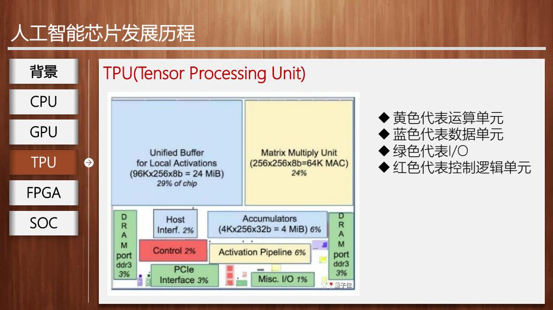
人工智能芯片发展历程 背景 TPU(Tensor Processing Unit) CPU ◆黄色代表运算单元 GPU ◆蓝色代表数据单元 Unified Buffer Matrix Multiply Unit ◆绿色代表/O TPU for Local Activations (256x256x8b=64KMAC) (96Kx256x8b=24MiB) 24% ◆红色代表控制逻辑单元 29%of chip FPGA SOC Host Accumulators D KA Interf.2% (4Kx256x32b=4MiB)6% A M M port Control 2% Activation Pipeline 6% port ddr3 ddr3 3% PCle 3% Interface 3% Misc.I/O 1% 子位
人工智能芯片发展历程 TPU(Tensor Processing Unit) 黄色代表运算单元 蓝色代表数据单元 绿色代表I/O TPU 红色代表控制逻辑单元 背景 CPU GPU FPGA SOC