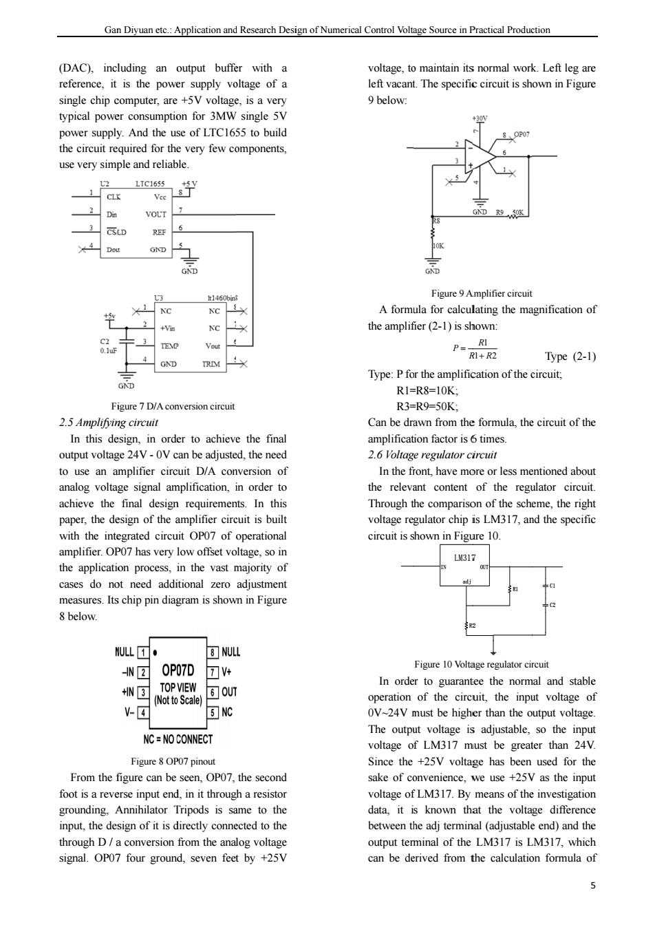
ch Design of Nu山 erica Control Source in Practica Production (DAC). is the an output buffer with voltage of a vacant.The specific circuit is shown in Figure single chip c 9 below typical power for 3MW single 5 power supply.And the of LTC1655 to build the circuit required for the very few components. use very simple and reliable. 4 OND Figure 9 Amplifier circuit d A formula for calculating the magnification of the amplifier (2-)is sho P=R+R Type (2-1) Type:Pfor the mplification of the circuit Figure 7D/A nversion Can be drawn from the formula,the circuit of the In this design,in order to achieve the fina amplification factor is 6 times output voltage 24V -OV can be adjusted,the need 2.6 Voltage regulator circuil to use an amplifier circuit D/A conversion of In the front,have more or less mentioned about analog voltage signal amplification,in order to the relevant content of the regulator circuit achieve the final design requirements.In this Through the comparison of the scheme,the right paper,the design of the amplifier circuit is built voltage regulator chip is LM317,and the specific with the integrated circuit OP07 of operational circuit is shown in Figure 10. amplifier.OP07 has very low offset voltage.so in L317 the application process,in the vast majority of cases do not need additional zero adiustment measures.Its chip pin diagram is shown in Figure 8 below 可MUL HW区0P07D 4 In th 州可 回oUn nd stable 0-24 hig The adjustable NC=NO CONNECT 301 31 be greater thar FigureOP07 pinou Since the +25V voltage has been used for the From the figure can be seen,OP07,the second sake of convenience,we use +25V as the inpu foot is a reverse input end,in it through a resistor voltage of LM317.By means of the investigation grounding.Annihilator Tripods is same to the data,it is known that the voltage difference input,the design of it is directly connected to the between the adi terminal (adjustable end)and the through D/a conversion from the analog voltage output temminal of the LM317 is LM317,which signal.OP07 four ground,seven feet by +25V can be derived from the calculation formula of 5
Gan (DAC), incl reference, it single chip c typical powe power supply the circuit re use very simp Fi 2.5 Amplifyin In this de output voltag to use an am analog voltag achieve the paper, the de with the inte amplifier. OP the applicatio cases do no measures. Its 8 below. From the f foot is a reve grounding, A input, the des through D / a signal. OP07 n Diyuan etc.: A luding an o is the powe computer, are er consumptio y. And the us quired for the ple and reliab igure 7 D/A con ng circuit esign, in orde ge 24V - 0V c mplifier circ ge signal am final design esign of the a egrated circu P07 has very l on process, i ot need addi s chip pin diag Figure 8 OP figure can be erse input end Annihilator T sign of it is d a conversion 7 four ground Application and output buffe er supply vo +5V voltage on for 3MW se of LTC165 e very few co ble. nversion circuit er to achieve can be adjuste cuit D/A con mplification, i n requiremen amplifier circ uit OP07 of o low offset vo in the vast m itional zero gram is show P07 pinout seen, OP07, d, in it throug Tripods is sa directly conne from the anal d, seven feet d Research Desi er with a oltage of a e, is a very single 5V 55 to build omponents, e the final ed, the need nversion of in order to nts. In this cuit is built operational oltage, so in majority of adjustment wn in Figure the second h a resistor ame to the ected to the log voltage t by +25V ign of Numerical Control Volta voltage, to left vacant 9 below: A formu the amplif Type: P fo R1= R3= Can be dra amplificat 2.6 Voltag In the fr the releva Through t voltage reg circuit is s In orde operation 0V~24V m The outpu voltage o Since the sake of co voltage of data, it i between th output term can be de age Source in P o maintain its t. The specific Figure 9 Am ula for calcul fier (2-1) is sh r the amplific =R8=10K; =R9=50K; awn from the ion factor is 6 e regulator ci ront, have mo ant content he compariso gulator chip i hown in Figu LM317 IN adj R2 Figure 10 Volta r to guarante of the circu must be highe ut voltage is f LM317 mu +25V voltag onvenience, w f LM317. By s known tha he adj termin minal of the erived from t R P = Practical Produc s normal work c circuit is sh Amplifier circuit lating the ma hown: cation of the c e formula, the 6 times. ircuit ore or less me of the regu on of the sche is LM317, an ure 10. 7 OUT 2 R1 age regulator cir tee the norm uit, the inpu er than the o s adjustable, must be great ge has been we use +25V means of the at the volta nal (adjustable LM317 is L the calculatio 1 2 1 R R R + ction 5 k. Left leg are own in Figure agnification o Type (2-1 circuit; e circuit of the entioned abou ulator circuit eme, the righ nd the specific C1 C2 rcuit mal and stable ut voltage o utput voltage so the inpu ter than 24V used for the V as the inpu e investigation ge difference e end) and the LM317, which on formula o 5 e e of ) e ut t. ht c e of e. ut V. e ut n e e h of

The English Proceedings of the College of nstrumentation&Electrical University.in the Second Half of 2015 the of shown in the program design of the micro level,pulse type formula(2-2). source includes the following several Uo=125*0+2 aspects:first,we must drive the single chip RI ype(2-2) microcomputer,which can output a PWM drive signal.Secondly,the digital signal is converted Type:Uout for LM317output voltage: into analog signal,then the output circuit is set RI for the adi end to the output of the up. resistance,that is,R; 3.2 Program block diagram R2 adj to the ground resistance,that is,the The flow chart of the program is shown in R2in the picture. Figure 12 below. 2 7 kevboard module As the final design requirement is to make the output pulse voltage waveform amplitude and pulse width can be adiusted so in order to facilitate control and the are ing.in Define the variabks and e specific calculate the caraneters show Enable LTC1655 to complete DA corversioo Figure l1 Kevboard circuit As shown above,due to the single chip ATmegal6 its PC port has a built-in N programmable pull resistor can be controlled b software programming to pull the resistor is effective or invalid.so there is no end the top of the al6 port of the PC port.as Figure 12 Program flow chart pull the PC 33 Princinles this led by need tage am cy,pulse The first is to the initial programming you can var achieve the above functions that th signal to normal drive every level of the device 3 SOFTWARE DESIGN SYSTEM to ensure that each component can work properly which is the most important basis for 3.I Program design programming.The second is to achieve the output Because it is the numerical control voltage pulse voltage amplitude,frequency and pulse source.so this design,in addition to the need for width can be adjusted.To achieve this,the first to hardware circuit,but also the need to complete use an if statement to determine whether a key is the design of the software to meet the pressed,if no key is pressed is out of the loop,ifa requirements of the final target.In this design,the key is pressed,the next step of judgment,if a key
The English 6 the output v formula (2-2) Type: Uout fo R1 for resistance, th R2 adj R2 in the pict 2.7 Keyboard As the fina output puls frequency an order to fac through softw achieve its n keyboard of Figure11. As shown ATmega16 programmabl software pro effective or i the top of ATmega16 p software prog pull of the controlled by frequency, pu through rea achieve the a 3 SOFTWARE 3.1 Program Because it source, so th hardware cir the design requirements Uo h Proceedings o voltage of 1. ). for LM317 ou r the adj end hat is, R1; to the groun ture. d module al design requ se voltage nd pulse width ilitate contro ware program numerical val f the specific Figure 11 Keyb n above, du its PC p le pull resisto ogramming t invalid, so th the resistor port of the P gramming to effective. y the output p ulse width of asonable pro above function DESIGN SYST design t is the num is design, in rcuit, but also of the so s of the final t out =1.25*( of the College o .25V, as sho utput voltage; d to the out nd resistance, uirement is to waveform h can be adju ol and the k mming, in the ue can be ad c circuit as board circuit ue to the s port has a or can be con to pull the ere is no con r, but direct PC port, as lo pull the PC p Six key sw pulse voltage the increase o ogramming, ns. TEM merical contr addition to th o the need to oftware to target. In this ) 1 2 (1 R R + f Instrumentatio own in the Type (2-2) tput of the that is, the o make the amplitude, usted, so in key switch, software to djusted, the shown in ingle chip a built-in ntrolled by resistor is nnection on tly to the ong as the port on the witches are amplitude, or decrease you can rol voltage he need for o complete meet the design, the on & Electrical Engineering, J program d voltage so aspects: f microcom signal. Se into analo up. 3.2 Progra The flo Figure 12 3.3 Princip In this consider t issues. Th the variou to ensure t signal to n to ensure t which is programm pulse volt width can use an IF pressed, if key is pres Jilin University, design of the ource includ first, we mu puter, which condly, the d og signal, the am block diag ow chart of t below. Figure 12 Pro ples of progra process de the following e first is to co us ports and t that the micro normal drive that each com s the mos ming. The seco tage amplitu be adjusted. statement to d f no key is pre ssed, the next , in the Second e micro leve des the follo ust drive the can output a digital signal en the output gram the program ogram flow cha am operation esign tasks, g two aspects onsider the in the definition ocontroller ou every level mponent can w st important ond is to achie ude, frequenc To achieve th determine wh essed is out o t step of judg Half of 2015 el, pulse type owing severa e single chip a PWM drive l is converted t circuit is se is shown in art the need to s of the main nitialization o n of variables ut of the drive of the device work properly t basis fo eve the outpu cy and pulse his, the first to hether a key i f the loop, if a ment; if a key e al p e d et n o n of s, er e, y, or ut e o s a y
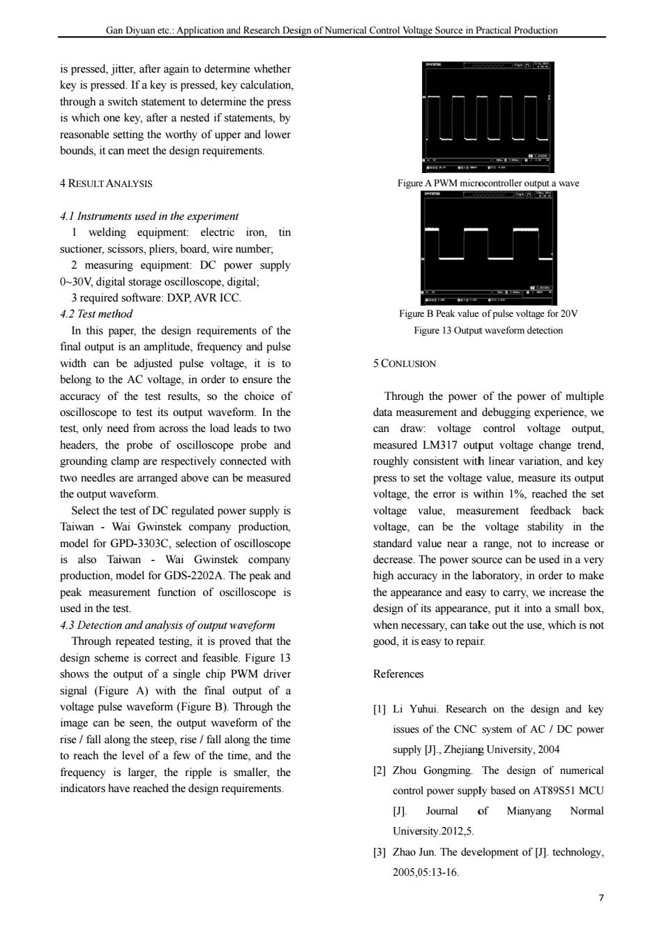
Gan Research Design of Numerica Control olge Source in Practical Production is pressed.again to deterine whethe key is presse t a key is pres through a switch ment to determine the press is which one key,after a nested if statements,by easonable setting the worthy of upper and lower bounds,it can meet the design requirements. 4 RESULT ANALYSIS Figure A PWM microcontroller ouput a ave 4.1 Instruments used in the experiment 1 welding equipment:electric iron,tin suctioner.scissors,pliers,board,wire number. 2 measuring equipment:DC power supply 0-30V digital storage oscilloscope.digital: 3 required software:DXP.AVR ICC. 4.2 Test method Figue B Peak value of pulse voltage for 20V In this paper,the design requirements of the Figure 1 Output waveform detection final output is an amplitude.fr and n width can he a ted pulse 5 CONLUSION belong to of the tes res so the Through the power of the power rof multipl est I deb gging experience,we ,only need fro om acro the load leads to two ca voltage contr voltage outpu headers,the probe of oscilloscope probe and measured LM317 output voltage change trend grounding clamp are respectively connected with roughly consistent with linear variation,and key two needles are arranged above can be measured press to set the voltage value,measure its output the output waveform. voltage,the error is within 1%.reached the set Select the test of DC regulated power supply is voltage value,measurement feedback back Taiwan-Wai Gwinstek company production, voltage,can be the voltage stability in the model for GPD-3303C selection of oscilloscone standard value near a range,not to increase or is also Taiwan Wai Gwinstek compan decrease.The power source can be used in a very production,model for GDS-2202A.The peak and high accuracy in the laboratory,in order to make peak measurement function of oscilloscope is the appearance and easy to carry.we increase the used in the test design of its appearance,put it into a small box. e when necessary,can take out the use,which is not design scheme is corre and feasible.Figure 13 the chip PWM dr References signal (Fig A)wi h tput o m (Figure B)Through [1]Li Yuhui.Research on the design and key can be seen. avelorm of th issues of the CNC system of AC/DC power along th eep,rise /fall along the to reach the level of supply [J]..Zhejiang University.2004 few of the time,and the frequency is larger,the ripple is smaller.the 2]Zhou Gongming.The design of numerical indicators have reached the design requirements. control power supply based on AT89S51 MCU of Mianyang Normal University.2012,5. 3]Zhao Jun.The development of [technology. 2005.05:13-16
Gan is pressed, jit key is pressed through a sw is which one reasonable se bounds, it can 4 RESULT AN 4.1 Instrumen 1 weldin suctioner, sci 2 measuri 0~30V, digita 3 required 4.2 Test meth In this pap final output i width can b belong to the accuracy of oscilloscope test, only nee headers, the grounding cla two needles a the output wa Select the Taiwan - W model for GP is also Tai production, m peak measur used in the te 4.3 Detection Through re design schem shows the ou signal (Figur voltage pulse image can b rise / fall alon to reach the frequency is indicators hav n Diyuan etc.: A tter, after aga d. If a key is witch statemen e key, after a etting the wor n meet the de NALYSIS nts used in the ng equipmen issors, pliers, ing equipme al storage osc software: DX hod per, the desi is an amplitud be adjusted p e AC voltage the test res to test its ou ed from acros probe of o amp are resp are arranged aveform. test of DC re Wai Gwinstek PD-3303C, s iwan - Wa model for GD rement funct est. n and analysis epeated testin me is correct utput of a si re A) with e waveform ( e seen, the o ng the steep, level of a fe s larger, the ve reached th Application and ain to determin pressed, key nt to determin nested if stat rthy of upper esign requirem e experiment nt: electric board, wire n ent: DC pow illoscope, dig XP, AVR ICC gn requireme de, frequency pulse voltage e, in order to sults, so the utput wavefo ss the load le oscilloscope ectively conn above can be egulated powe k company p election of o ai Gwinstek DS-2202A. Th tion of oscil s of output wa ng, it is prov and feasible. ingle chip PW the final ou (Figure B). T output wavefo rise / fall alon ew of the tim ripple is sm he design requ d Research Desi ne whether calculation, ne the press tements, by r and lower ments. iron, tin number; wer supply gital; . ents of the y and pulse e, it is to ensure the choice of orm. In the eads to two probe and nected with e measured er supply is production, scilloscope company he peak and lloscope is aveform ved that the . Figure 13 WM driver utput of a Through the form of the ng the time me, and the maller, the uirements. ign of Numerical Control Volta Figure Figur F 5 CONLUS Through data meas can draw measured roughly co press to se voltage, th voltage v voltage, c standard v decrease. T high accur the appear design of when nece good, it is Reference [1] Li Yu issues supply [2] Zhou contro [J]. Unive [3] Zhao J 2005,0 age Source in P e A PWM micro re B Peak value igure 13 Output ION h the power urement and w: voltage LM317 outp onsistent with et the voltage he error is w value, meas can be the value near a The power so racy in the la rance and eas its appearanc essary, can tak easy to repair s uhui. Researc of the CNC y [J]., Zhejiang Gongming. ol power suppl Journal o rsity.2012,5. Jun. The deve 05:13-16. Practical Produc ocontroller outp of pulse voltag t waveform dete of the powe debugging ex control vol put voltage c h linear varia e value, meas within 1%, re surement fee voltage sta range, not t ource can be u aboratory, in o sy to carry, w ce, put it into ke out the use ir. ch on the de system of AC g University, 2 The design ly based on A of Mianya elopment of [J ction 7 put a wave ge for 20V ection er of multiple xperience, we ltage output change trend ation, and key sure its outpu eached the se edback back ability in the to increase o used in a very order to make we increase the o a small box e, which is no esign and key C / DC powe 2004 of numerica AT89S51 MCU ang Norma J]. technology 7 e e t, d, y ut et k e or y e e x, ot y er al U al y

The English Proceedings of the College of Insrumenation&Electrical Engineering.Jin University.in the Second Half of 2015 [4]left x g.Based on DC voltage source AVR microcontroller design of microcomputer and application.2012. [5]Li Shuo.Design and research of remote wireless monitoring system [J].Nankai University,06 8
The English Proceedings of the College of Instrumentation & Electrical Engineering, Jilin University, in the Second Half of 2015 8 [4] left x g. Based on DC voltage source AVR microcontroller design of [J]. microcomputer and application, 2012, [5] Li Shuo. Design and research of remote wireless monitoring system [J]. Nankai University, 2006
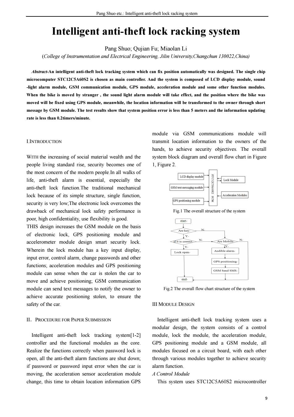
Pang Shuo anti-the lock racking syste Intelligent anti-theft lock racking system Pang Shuo;Qujian Fu,Miaolan L (College of Instrumentation and Electrical Engineering.Jilin University.Changchun 130022.China) Abstract-An intelligent anti-theft lock tracking system which can fix position automatically was designed.The single chip omputer STC12C5A60S2 is chosen as main controller.and the system is composed of lcd display module.sound ight alar module,GSM communication module,GPS module, module and other When the bike is moved by stranger,the sound light alarm module will take and the position where the bike wa moved will be fixed using GPS module,meanwhile,the location information will be transformed to the owner through short message by GSM module.The test results show that system position error is less than 5 meters and the information updating rate is less than 0.2timers/minute. module via GSM communications module will I.INTRODUCTION transmit location information to the owners of the hands,to achieve security objectives.The overall WrH the increasing of social material wealth and the system block diagram and overall flow chart in Figure s one of 1,Figure2. the most of the mode walk LCD dioplay modale life,anti-theft alarm is essential,especially the anti-theft lock function The traditional mechanical lock because of its simple structure.single function security is very low,The electronic lock ov ercomes the draw back of me safety performance is poor,high confidentiality,use flexibility is good THIS design increases the GSM module on the basis of electronic lock.GPS positioning module and accelerometer module design smart security lock Wherein the lock module has a key input display input error,control alarm,change passwords and othe OPS P functions:acceleration modules and GPS positioning module can sense when the car is stolen the car to move and achieve positioning:GSM communication text messages to notify the owner Fig The overall flow chart structure of the syster achieve accurate positioning stolen,to ensure the safety of the car. III MODULE DESIGN IL PROCEDURE FOR PAPER SUBMISSION Intelligent anti-theft lock tracking system uses a modular design,the system consist of a Intelligent anti-theft lock tracking system[1-2] module,lock the module,the acceleration module controller and the functional modules as the core. GPS positioning module and a GSM module,al Realize the functions correctly when password lock is modules focused on a circuit board,with each other open,all the anti-theft alarm functions are shut down. through various modules together to achieve security alarm function moving.the acceleration sensoracceleration modul change.this time to obtain location information GPS This system uses STC12C5A60S2 microcontroller
Pang Shuo etc.: Intelligent anti-theft lock racking system 9 Intelligent anti-theft lock racking system Pang Shuo; Qujian Fu; Miaolan Li (College of Instrumentation and Electrical Engineering, Jilin University,Changchun 130022,China) Abstract-An intelligent anti-theft lock tracking system which can fix position automatically was designed. The single chip microcomputer STC12C5A60S2 is chosen as main controller. And the system is composed of LCD display module, sound -light alarm module, GSM communication module, GPS module, acceleration module and some other function modules. When the bike is moved by stranger , the sound light alarm module will take effect, and the position where the bike was moved will be fixed using GPS module, meanwhile, the location information will be transformed to the owner through short message by GSM module. The test results show that system position error is less than 5 meters and the information updating rate is less than 0.2timers/minute. I.INTRODUCTION WITH the increasing of social material wealth and the people living standard rise, security becomes one of the most concern of the modern people.In all walks of life, anti-theft alarm is essential, especially the anti-theft lock function.The traditional mechanical lock because of its simple structure, single function, security is very low;The electronic lock overcomes the drawback of mechanical lock safety performance is poor, high confidentiality, use flexibility is good. THIS design increases the GSM module on the basis of electronic lock, GPS positioning module and accelerometer module design smart security lock. Wherein the lock module has a key input display, input error, control alarm, change passwords and other functions; acceleration modules and GPS positioning module can sense when the car is stolen the car to move and achieve positioning; GSM communication module can send text messages to notify the owner to achieve accurate positioning stolen, to ensure the safety of the car. II.PROCEDURE FOR PAPER SUBMISSION Intelligent anti-theft lock tracking system[1-2] controller and the functional modules as the core. Realize the functions correctly when password lock is open, all the anti-theft alarm functions are shut down; if password or password input error when the car is moving, the acceleration sensor acceleration module change, this time to obtain location information GPS module via GSM communications module will transmit location information to the owners of the hands, to achieve security objectives. The overall system block diagram and overall flow chart in Figure 1, Figure 2. Fig.1 The overall structure of the system Fig.2 The overall flow chart structure of the system III MODULE DESIGN Intelligent anti-theft lock tracking system uses a modular design, the system consists of a control module, lock the module, the acceleration module, GPS positioning module and a GSM module, all modules focused on a circuit board, with each other through various modules together to achieve security alarm function. A Control Module This system uses STC12C5A60S2 microcontroller