CONTENTS Application and Research Design of Numerical Control Voltage Source in Practical Production. ..Gan Diyuan;Huang Linshu;Tan Hao 1 Intelligent anti-theft lock racking system ......................Pang Shuo;Qujian Fu;Miaolan Li 9 Smart Home based on Raspberry Pi ..Liu Jiwei;Liu Mengchen;Gao Ranran 15 Distributed Wirele Monitoring System of Factory Machinery Temperature. .......Cao zhan-peng:Zhou bo;Mu-tingting 21 The design of semiconductor laser modulation circuit based on DDS technology. .Jiang yanhui;Sun chaofan;Chen wenxing 27 Life rescue system based on CC1101... ....Gao Jiafei;Deng Wen;Sun Liyuan 35 Design of intelligent guide rod based on the infrared alarm. .XIE Yantong:CUI Yuqi;DENG Qitian 41 Design and implementation of a movement monitoring system based on the human body sensor and android technology. Caijing:Zhourui;Tianruyun;Liulei 45 Design and implementation of speech presenter microphone based on LD3320.. Liang Yi-gang:Huang Ji-wei;Liu Shi-bin 1 Portable positioning device for field wiring of electromagnetic field .....Wang Haoyu;Zhang Caihong:Ren Wei 57 Design and Implementation of Micro-quality PVDF-based Weighing System....... ......Peng Cong;Liu Bo;Yan Jiaqi 63 The research and design of the single oil well tank of information monitoring and control system... .......Cai Jing:Wang Qian;Yang Yujing:Li Chang 67 The design of bluetooth entrance control system..... Qi Wang:Chao Yang:Yiguang Bao 71 Ultrasonic Ranging Based on blind navigation Headphones. .....Xiaotong Cui;Zhaofeng Zhang:Xulei Wang 77 The design of a tracing luggage robot based on the ultrasonic ranging.... Ning Hong-yang,Wang Ti-kuo,Zhao Yi 81
I CONTENTS Application and Research Design of Numerical Control Voltage Source in Practical Production .......... .............................................................................................. Gan Diyuan; Huang Linshu; Tan Hao 1 Intelligent anti-theft lock racking system ................................................................................................ .................................................................................................. Pang Shuo; Qujian Fu; Miaolan Li 9 Smart Home based on Raspberry Pi ........................................................................................................ ............................................................................................ Liu Jiwei; Liu Mengchen; Gao Ranran 15 Distributed Wirele Monitoring System of Factory Machinery Temperature .......................................... ............................................................................................. Cao zhan-peng; Zhou bo; Mu-tingting 21 The design of semiconductor laser modulation circuit based on DDS technology ................................. ...................................................................................... Jiang yanhui; Sun chaofan; Chen wenxing 27 Life rescue system based on CC1101 ...................................................................................................... .................................................................................................. Gao Jiafei; Deng Wen; Sun Liyuan 35 Design of intelligent guide rod based on the infrared alarm .................................................................... ........................................................................................... XIE Yantong; CUI Yuqi; DENG Qitian 41 Design and implementation of a movement monitoring system based on the human body sensor and android technology ................................................................................................................................... ................................................................................................. Caijing; Zhourui; Tianruyun; Liulei 45 Design and implementation of speech presenter microphone based on LD3320 .................................... ....................................................................................... Liang Yi-gang; Huang Ji-wei; Liu Shi-bin 51 Portable positioning device for field wiring of electromagnetic field ..................................................... .......................................................................................... Wang Haoyu; Zhang Caihong; Ren Wei 57 Design and Implementation of Micro-quality PVDF-based Weighing System ....................................... .......................................................................................................... Peng Cong; Liu Bo; Yan Jiaqi 63 The research and design of the single oil well tank of information monitoring and control system ....... .................................................................................. Cai Jing; Wang Qian; Yang Yujing; Li Chang 67 The design of bluetooth entrance control system .................................................................................... ................................................................................................. Qi Wang; Chao Yang; Yiguang Bao 71 Ultrasonic Ranging Based on blind navigation Headphones ................................................................... ................................................................................... Xiaotong Cui; Zhaofeng Zhang;Xulei Wang 77 The design of a tracing luggage robot based on the ultrasonic ranging ................................................... ......................................................................................... Ning Hong-yang; Wang Ti-kuo; Zhao Yi 81
Gan Diy App and Re ch Design of Numerical Control Voltage Source n Pr al Production Application and Research Design of Numerical Control Voltage Source in Practical Production Gan Diyuan;Huang Linshu;Tan Hao College of Instrumentation and Electrical Engineering.University Changchun 130026 Abstract-With the rapid development of science and technology,power technology has increasingly become a practical and comprehensive engineering technology.widely used in all walks of life,and the numerical control power supply technology is articarly important.Microseond,pulse type umerical c is by thei of the digital utp p width can be adjusted.Thi cal control voltage source,in es the design and implementation of the micro-level,pulse typ nerical control voltage source..The digital control technology of single chip microcomputer is integrated into the design o voltage souree,reasonably and effectively.It makes the control of the power supply is more simple and implementation of the power supply of CNC. rds-Numerical control:ATmega16 single chip omputer:D/A conversion:A/D conversion supply system has been to the beginning of INTRODUCTION twenty-first Century,more advanced fourth generation distributed power supply structure,the ALONG with the development of science and power industry is facing a new challenge,that is. technology,the modern information technology the existing system in the embedded power has provided a more broad development platform supply digital control and intelligent systems.The for the development of power electronics numerical control voltage source is from the last technology.at the same time.the power supply century 80's only then truly starts to develop technology has been put forward more stringen During this period.the entire system of powe standards and requirements.Power supply is a electronics theory began to gradually establish men and continuously improve.in a long time.the numerical control yol source technology has long-term ent in the 90 whole system,this is a nductor manufacturers to develop on the nun .Numerical out at that tir of the ofsimlhtion& gy nowadays,and it is widely s in a osition,so thi logy ca e w source is usually the rch on the nume erical votag band switch and potentiometer to adjust the started late,and in the late voltage source.the voltage value of the voltage ninety's of the last century,under the Nationa meter to indicate the size of the voltage value.so Natural Science Foundation of China,Zhejiang that the reading accuracy is not high.and easy to University.North China Electric Powe wear.Compared with the traditional voltage University and other colleges and universities source.the numerical control voltage source have launched this aspect of the basic theoretical based on single chip microcomputer control has research. the characteristics of easy control,high reliability Numerical control power supply technology and high accuracy.It is a good solution to the has been develoned from 1980s to now but its problem of the traditional voltage source products still exist in this way or that.such as its From the first generation of the 80's in the last high resolution.low reliability.etc..It can be seer ,the first eneration ofdistributed ower that the development direction of the numerical 1
Gan Diyuan etc.: Application and Research Design of Numerical Control Voltage Source in Practical Production 1 Application and Research Design of Numerical Control Voltage Source in Practical Production Gan Diyuan; Huang Linshu; Tan Hao (College of Instrumentation and Electrical Engineering, Jilin University Changchun 130026) Abstract-With the rapid development of science and technology, power technology has increasingly become a practical and comprehensive engineering technology, widely used in all walks of life, and the numerical control power supply technology is particularly important. .Microsecond, pulse type numerical control voltage source is controlled by the size of the digital output voltage. The output pulse voltage amplitude, pulse width, frequency can be adjusted. This paper studies the development of numerical control voltage source, introduces the design and implementation of the micro - level, pulse type numerical control voltage source,.The digital control technology of single chip microcomputer is integrated into the design of voltage source, reasonably and effectively .It makes the control of the power supply is more simple and implementation of the power supply of CNC. Key words-Numerical control; ATmega16 single chip microcomputer; D/A conversion; A/D conversion INTRODUCTION ALONG with the development of science and technology, the modern information technology has provided a more broad development platform for the development of power electronics technology, at the same time, the power supply technology has been put forward more stringent standards and requirements. Power supply is a very important part of the electronic equipment, the traditional power in the work of the error, will have a considerable impact on the accuracy of the whole system, this is a more stringent requirements on the numerical control voltage source. Numerical control voltage source is one of the equipments which is often used in the electronic technology nowadays, and it is widely used in various industries. The traditional voltage source is usually the band switch and potentiometer to adjust the voltage source, the voltage value of the voltage meter to indicate the size of the voltage value, so that the reading accuracy is not high, and easy to wear. Compared with the traditional voltage source, the numerical control voltage source based on single chip microcomputer control has the characteristics of easy control, high reliability and high accuracy. It is a good solution to the problem of the traditional voltage source. From the first generation of the 80's in the last century, the first generation of distributed power supply system has been to the beginning of twenty-first Century, more advanced fourth generation distributed power supply structure, the power industry is facing a new challenge, that is, the existing system in the embedded power supply digital control and intelligent systems. The numerical control voltage source is from the last century 80 's only then truly starts to develop. During this period, the entire system of power electronics theory began to gradually establish and continuously improve, in a long time, the numerical control voltage source technology has a long-term development; in the 90's, semiconductor manufacturers to develop a numerical control voltage source management technology, but at that time, this technology has been used in a wide range of simulation control scheme, which is in a inferior position, so this technology can not be widely used. The research on the numerical control voltage source in China started late, and in the late ninety's of the last century, under the National Natural Science Foundation of China, Zhejiang University, North China Electric Power University and other colleges and universities have launched this aspect of the basic theoretical research. Numerical control power supply technology has been developed from 1980s to now, but its products still exist in this way or that, such as its high resolution, low reliability, etc.. It can be seen that the development direction of the numerical

The English Proceedings of the College of&Electrical Engineering.n University.in the Second Half of 2015 sply is mainly to improve the +2.5Vvoltage.As long as the AD7802 pin intoa above shortcomings.at the same time,on this V voltage.it can be programmed to make its 6 basis,we must continue to innovate and reform foot output of a 2.5V or 3.0V voltage,its accuracy is 2.5V+ImV or 3+1mV.The specific 1 OVERALL SCHEME SELECTION circuit is shown in Figure 2. 1.I The overall design scheme of the voltage source of the pulse type numerical control AC voltage input 100V--240V by a switching power supply output 5V DC voltage to the AVR MCU power supply,the output signal to the A78 microcontroller to drive the D/A conversion part, while using the AVR microcontroller internal oscillator provides a clock signal for it,then the signal for analog then to the circuit of pow make signal i igre 2 AD780 and th nea voltage reg t1460bin8-2.5 circu voltag produ +2.5V chip pro tage.Lt14 to the du mmy loa fte you can ma n and small package siz t this is an ope whic micro power b gap reterence,very signal output to prec voltage regulator. And h a MOS pipe,to control the switch tube guided by It1460bin8-2.5 does not need to outpu pulse width modulation on time so as to control compensation capacitor,and it is still stable the output voltage of the MOS tube,only need to capacitive load.Its specific wiring diagram is be connected with the dummy load can be shown in Figure 3: completed in a closed-loop system.In the end. Lt1460bing-2.5 through the software programming the voltage source output pulse voltage amplitude frequenc and pulse width can be reached by the reasonable setting of several soft switch,which can reach the final requirements.The overall structure diagram is shown in Figure 1. e 3.2 5 wirin t)pa h。 abov sche One of the ive the AD780 input tage,an s 8 ng,you can output a relatively st voltage.Scheme 2 as long as to It1460bin8-2.3 FigureOverall structure diagram provide input voltage of a 3.4V-20V and 1.2 Generation +2.5V scheme selection between the second heel legs connected with a In order to guarantee the normal operation of 0.luF capacitor,you can generate a stable+2.5V the circuit,it is needed to provide a+2.5V point output voltage.Compared with the scheme.the voltage to its part of the circuit and now there are circuit is much simpler and requires only one two options to choose from. capacitor,and the output voltage is stable,and the Program 1:the high precision reference voltage error is small.To sum up,through the comparison source AD is produced by AD780 to provide the program two more in line with the design
The English Proceedings of the College of Instrumentation & Electrical Engineering, Jilin University, in the Second Half of 2015 2 control power supply is mainly to improve the above shortcomings, at the same time, on this basis, we must continue to innovate and reform. 1 OVERALL SCHEME SELECTION 1.1 The overall design scheme of the voltage source of the pulse type numerical control AC voltage input 100V -- 240V by a switching power supply output 5V DC voltage to the AVR MCU power supply, the output signal to the microcontroller to drive the D/A conversion part, while using the AVR microcontroller internal oscillator provides a clock signal for it, then the output signal for analog signals; then to the amplifying circuit of power supply, make simulation the output voltage signal is amplified by the amplifying circuit as required; and then the amplified voltage through the voltage regulator circuit, you can get a stable output voltage, connected to the dummy load after you can make it work, but this is an open loop structure, which requires the chip outputs a PWM signal output to a MOS pipe, to control the switch tube guided by pulse width modulation on time so as to control the output voltage of the MOS tube, only need to be connected with the dummy load can be completed in a closed-loop system. In the end, through the software programming, the voltage source output pulse voltage amplitude, frequency and pulse width can be reached by the reasonable setting of several soft switch, which can reach the final requirements. The overall structure diagram is shown in Figure 1. Figure 1 Overall structure diagram 1.2 Generation +2.5V scheme selection In order to guarantee the normal operation of the circuit, it is needed to provide a +2.5V point voltage to its part of the circuit, and now there are two options to choose from. Program 1: the high precision reference voltage source AD is produced by AD780 to provide the +2.5V voltage. As long as the AD7802 pin into a 5V voltage, it can be programmed to make its 6 foot output of a 2.5V or 3.0V voltage, its accuracy is 2.5V + 1mV or 3 + 1mV. The specific circuit is shown in Figure 2. Figure 2 AD780 wiring mode Scheme two: using linear (linear) lt1460bin8-2.5 chip production company to produce +2.5V voltage. Lt1460bin8-2.5 is a low power, high precision and small package size of the micro power bandgap reference, very suitable for precision voltage regulator. And the lt1460bin8-2.5 does not need to output compensation capacitor, and it is still stable capacitive load. Its specific wiring diagram is shown in Figure 3: Figure 3 lt1460bin8-2.5 wiring mode Scheme comparison: the above two schemes can output 2.5V voltage. One of the solutions is to give the AD780 input 5V voltage, and its 8 foot floating, you can output a relatively stable +2.5V voltage. Scheme 2 as long as to lt1460bin8-2.5 provide input voltage of a 3.4V~20V and between the second heel legs connected with a 0.1uF capacitor, you can generate a stable + 2.5V output voltage. Compared with the scheme, the circuit is much simpler and requires only one capacitor, and the output voltage is stable, and the error is small. To sum up, through the comparison program two more in line with the design
Gan Diyuan and Research Design of Numeric Control Voltage the final choice of a program Icore chip selection 2 WORKING PRINCIPLE OF EACH UNIT CIRCUIT regulator power supply LM317 is adjustable 3-terminal voltage 2.I Control section regulator power supply,it is possible to The design of the numerical control part is continuous uninterrupted output can be 1.2 to based on the microcontroller ATmegal6 as the 37V ADJUSTABLE DC voltage,but the only fly core to complete.ATmegal6 pin diagram is in the ointment is it can output to a continuous shown in Figure 4 below.ATmegal6 is a high tone adjustable positive voltage,not negative speed,low power,8 bit CMOS microcontroller output voltage.LM317 regulator contains an based on the enhanced RISC AVR structure internal Overcurrent protection circuit and designed by ATMEL company.Because of its overheat protection circuit;the output voltage advanced instruction set and single clock cycle regulating circuit is composed of a resistor and a instruction execution time.the contradiction sliding rheostat between power consumption and processing Program two:the use of Cw78XX series three speed inal voltage regulator In this design,the toprovide eries a driv signal for each (V stabilized it is by the ure that the circui signal,to hre fee wh the th e MOS tube.Bel will introduce some of th ca ca ATmegal6 inf ve a with the can improve th a very typical chip,its main leatures are as load at the instant of impact,also can keep good follows waveform.And the stability of the circuit using RISC core with advanced LOW architecture 78XX series is also relatively good.reliable.easy and Harvard architecture.it has the 1MIPS MHz to use,and the price is cheap.The input voltage high speed computing execution ability,with of the 78XX series voltage regulator module is independent program bus and data bus,mos 36V and the lowest input voltage is higher thar instruction execution cycle is a single instruction the output voltage 3V~4V. cycle which contains a large amount of Scheme comparison:the two schemes can be non-volatile memory program and data memory. used as the core chip of the construction of the The chip contains two reset circuit,which regulator circuit.LM317 is the three terminal includes 32 general-purpose working registers. adjustable regulator chip.the and it all works as static work.As input,it can be adjustable,adjustable is 1.2V- -37V:the current can be CW78XX series ATmegal6. which can regulator chip her MCU Bt. comp very little and th meg the abili high have a supe ove set and ·Sped on n circuit and adjust speripheral more simple .Be protectior circuit, s very tion to the ATmegal convenient,and compared with LM317,it can several major pins as well as the functions of its output negative voltage.But the output voltage of pins the CW78XX series is a fixed value and is not ATmegal6 pin diagram is shown in Figure 4 adjustable.In summary, with the design below,and the main function of the pin is requirements of this paper.the need for a three analyzed as follows: adjustable voltage regulator chip.so the program is more in line with the design requirements,so 3
Gan Diyuan etc.: Application and Research Design of Numerical Control Voltage Source in Practical Production 3 requirements, so the choice of scheme two. 1.3 Voltage regulator circuit core chip selection Scheme one: LM317 adjustable three terminal regulator power supply LM317 is adjustable 3-terminal voltage regulator power supply, it is possible to continuous uninterrupted output can be 1.2 to 37V ADJUSTABLE DC voltage, but the only fly in the ointment is it can output to a continuous tone adjustable positive voltage, not negative output voltage. LM317 regulator contains an internal Overcurrent protection circuit and overheat protection circuit; the output voltage regulating circuit is composed of a resistor and a sliding rheostat. Program two: the use of CW78XX series three terminal voltage regulator 78XX series are fixed three terminal voltage stabilized power supply, it is by the output (VO), input pin (VI) and ground anchor (GND) the three tube feet, wherein, the input end is connected to a capacitor can better filtering, waveform in order to achieve a better; output end is connected with the capacitor can improve the load at the instant of impact, also can keep good waveform. And the stability of the circuit using 78XX series is also relatively good, reliable, easy to use, and the price is cheap. The input voltage of the 78XX series voltage regulator module is 36V, and the lowest input voltage is higher than the output voltage 3V~4V. Scheme comparison: the two schemes can be used as the core chip of the construction of the regulator circuit. LM317 is the three terminal adjustable regulator chip, the output voltage adjustable, adjustable range is 1.2V~37V; the maximum current can be provided for 1.5A. CW78XX series is the three terminal fixed regulator chip, using it to build and the required peripheral components is very little, and the circuit has a flow protection circuit, over temperature protection circuit and adjust the protection circuit, the use is very reliable, convenient, and compared with LM317, it can output negative voltage. But the output voltage of the CW78XX series is a fixed value and is not adjustable. In summary, with the design requirements of this paper, the need for a three adjustable voltage regulator chip, so the program is more in line with the design requirements, so the final choice of a program. 2 WORKING PRINCIPLE OF EACH UNIT CIRCUIT 2.1 Control section The design of the numerical control part is based on the microcontroller ATmega16 as the core to complete. ATmega16 pin diagram is shown in Figure 4 below. ATmega16 is a high speed, low power, 8 bit CMOS microcontroller based on the enhanced RISC AVR structure designed by ATMEL company. Because of its advanced instruction set and single clock cycle instruction execution time, the contradiction between power consumption and processing speed can be reduced. In this design, the ATmega16 is used to provide a driving signal for each part of the circuit to ensure that the circuit can drive the normal; secondly, the output of the PWM signal, to drive the MOS tube. Below will introduce some of the ATmega16 information. ATmega16 is the AVR series microcontroller in a very typical chip, its main features are as follows: RISC core with advanced LOW architecture and Harvard architecture, it has the 1MIPS / MHz high speed computing execution ability, with independent program bus and data bus, most instruction execution cycle is a single instruction cycle, which contains a large amount of non-volatile memory program and data memory. The chip contains two reset circuit, which includes 32 general-purpose working registers, and it all works as static work. As input, it can be set to three state high impedance input or AVR. The above is about the characteristics of ATmega16, which can be seen from the comparison with other 8 - MCU Bit, Bit 8 - MC ATmega16 has the ability to have a super - reduced instruction set and high - speed operation, and its peripheral circuits are more simple. Below will be a brief introduction to the ATmega16 several major pins as well as the functions of its pins. ATmega16 pin diagram is shown in Figure 4 below, and the main function of the pin is analyzed as follows:
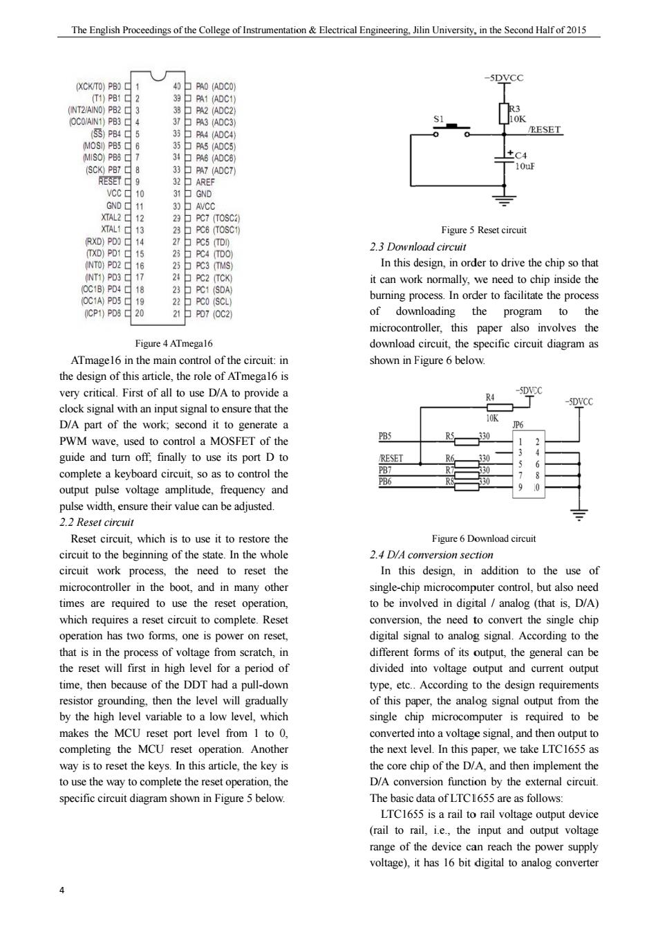
The English Proceedings of the College of&Electrical Engineering University.in the Second Half of 015 ESE Figure5 Reset circuit 2 3 Dmenload circuit In this design.in order to drive the chip so tha it can work n mally we need to chin inside th ing pro e In order to facilitate e the pr CP1 2 the the ontroller.this Figure 4 ATmegal6 downloadcicut.heae specific circuit diagram a shown in Figure 6below the d this First c F all t D/A to provide clock signa n an in gh I to ensure that th D/A part of the work to generate 阳5 PWM wave,used to control a MOSFET of the guide and turn off.finally to use its port D to RESET complete a keyboard circuit.so as to control the output pulse voltage amplitude,frequency and pulse width,ensure their value can be adjusted 22 Reset circuit Reset circuit which is to use it to restore the Figure 6 Download citcuit circuit to the beginning of the state.In the whole 2 dD/A couversion section circuit work process.the need to reset the In this design.in addition to the use o microcontroller in the boot,and in many othe single-chip mic computer control but also need the reset op to be involved in digital/analog (that is,D/A) complet rsion the need to chi n ha one is signal to ng to th is inth of s of its output h genera nig a pe outp outpu DDT had a pul Acc rding to o the design requirements ng,ther will grad analog signal ouput f by the high variable level,whi is required to b makes the MCl port level from I to 0. verted into a vo ltage signal,and then output to completing the MCU reset operation.Anothe the next level.In this paper,we take LTC1655 as way is to reset the keys.In this article.the key is the core chip of the D/A.and then implement the to use the way to complete the reset operation.the D/A conversion function by the external circuit. specific circuit diagram shown in Figure 5 below. The basic data of LTC1655 are as follows: LTC1655 is a rail to rail voltage output device (rail to rail.ie.the input and output voltage range of the device can reach the power supply voltage),it has 16 bit digital to analog converte
The English 4 ATmage16 the design of very critical. clock signal w D/A part of PWM wave, guide and tu complete a k output pulse pulse width, e 2.2 Reset circ Reset circu circuit to the circuit work microcontroll times are re which requir operation has that is in the the reset wil time, then be resistor grou by the high makes the M completing t way is to res to use the wa specific circu h Proceedings o Figure 4 AT 6 in the main f this article, t First of all t with an input the work; s used to con urn off; finall keyboard circ e voltage am ensure their v cuit uit, which is beginning of k process, th ler in the bo equired to us res a reset cir s two forms, e process of v ll first in hig ecause of the unding, then t level variable MCU reset p the MCU re et the keys. I ay to complete uit diagram sh of the College o Tmega16 control of the the role of AT to use D/A to signal to ensu second it to ntrol a MOSF ly to use its uit, so as to mplitude, freq value can be a to use it to f the state. In he need to oot, and in m se the reset rcuit to comp one is powe voltage from gh level for a e DDT had a the level wil e to a low le port level fro eset operation In this article e the reset ope hown in Figur f Instrumentatio e circuit: in Tmega16 is o provide a ure that the generate a FET of the port D to control the quency and adjusted. restore the n the whole reset the many other operation, plete. Reset er on reset, scratch, in a period of pull-down l gradually evel, which om 1 to 0, n. Another , the key is eration, the re 5 below. on & Electrical Engineering, J 2.3 Downl In this d it can wor burning pr of down microcont download shown in F 2.4 D/A co In this single-chip to be invo conversion digital sig different f divided in type, etc.. of this pa single ch converted the next le the core ch D/A conv The basic LTC165 (rail to ra range of t voltage), i Jilin University, Figure 5 load circuit design, in ord rk normally, w rocess. In ord nloading th roller, this circuit, the s Figure 6 below Figure 6 Do onversion sect design, in p microcomp olved in digit n, the need t gnal to analog forms of its o nto voltage o According t per, the analo ip microcom into a voltage evel. In this p hip of the D/A ersion functio data of LTC1 55 is a rail to ail, i.e., the the device ca it has 16 bit d , in the Second Reset circuit der to drive th we need to c der to facilita the program paper also specific circu w. ownload circuit ction addition to puter control, tal / analog to convert th g signal. Acc output, the g output and c to the design log signal ou mputer is re e signal, and paper, we take A, and then i on by the ex 1655 are as fo o rail voltage input and o an reach the digital to ana Half of 2015 he chip so tha hip inside the ate the proces m to the involves the uit diagram a t o the use o but also need (that is, D/A he single chip cording to the general can be current outpu requirement utput from the quired to be then output to e LTC1655 a implement the xternal circuit ollows: output device output voltage power supply alog converte at e s e e s of d A) p e e ut s e e o as e t. e e y er