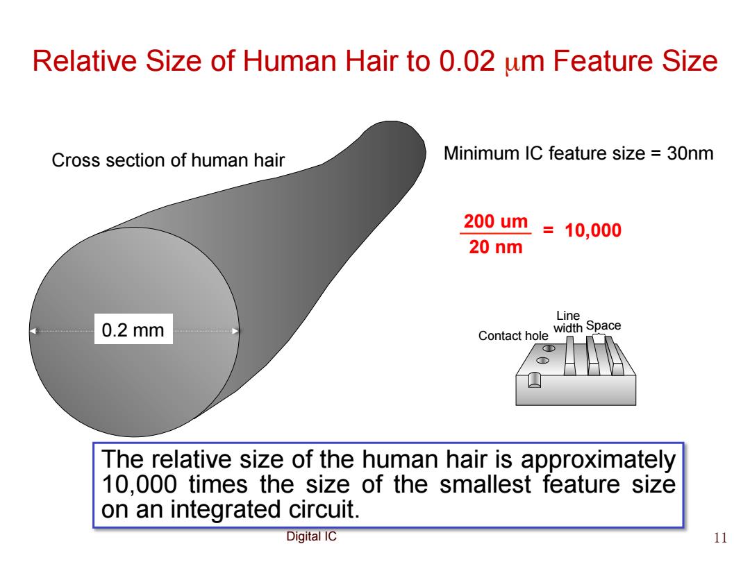
Relative Size of Human Hair to 0.02 um Feature Size Cross section of human hair Minimum IC feature size 30nm 200um =10,000 20 nm Line 0.2mm Contact hole width Space D The relative size of the human hair is approximately 10,000 times the size of the smallest feature size on an integrated circuit. Digital IC 11
Digital IC Relative Size of Human Hair to 0.02 µm Feature Size Contact hole Line width Space 0.2 mm Minimum IC feature size = 30nm The relative size of the human hair is approximately 10,000 times the size of the smallest feature size on an integrated circuit. Cross section of human hair 200 um 20 nm = 10,000 11
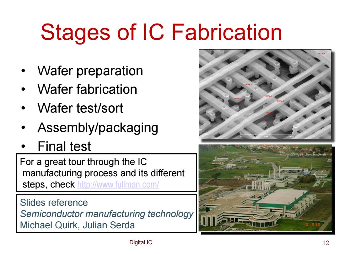
Stages of IC Fabrication Wafer preparation Wafer fabrication Wafer test/sort Assembly/packaging Final test For a great tour through the IC manufacturing process and its different steps,check http://www.fullman.com/ Slides reference Semiconductor manufacturing technology Michael Quirk,Julian Serda 01998 Digital IC 12
Digital IC Stages of IC Fabrication • Wafer preparation • Wafer fabrication • Wafer test/sort • Assembly/packaging • Final test For a great tour through the IC manufacturing process and its different steps, check http://www.fullman.com/ Slides reference Semiconductor manufacturing technology Michael Quirk, Julian Serda 12
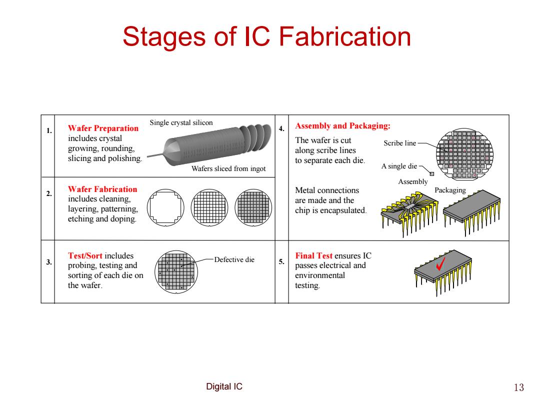
Stages of IC Fabrication Single crystal silicon 1. Wafer Preparation 4. Assembly and Packaging: includes crystal The wafer is cut Scribe line growing,rounding, along scribe lines slicing and polishing. to separate each die. Wafers sliced from ingot A single die Assembly 2. Wafer Fabrication Metal connections Packaging includes cleaning, are made and the layering,patterning, chip is encapsulated. etching and doping. Test/Sort includes Defective die Final Test ensures IC probing,testing and 5. passes electrical and sorting of each die on environmental the wafer. testing. Digital IC 13
Digital IC Stages of IC Fabrication Wafer Preparation includes crystal growing, rounding, slicing and polishing. Assembly and Packaging: The wafer is cut along scribe lines to separate each die. Metal connections are made and the chip is encapsulated. Wafer Fabrication includes cleaning, layering, patterning, etching and doping. Test/Sort includes probing, testing and sorting of each die on the wafer. Final Test ensures IC passes electrical and environmental testing. Defective die 1. 2. 3. Scribe line A single die Assembly Packaging 4. 5. Wafers sliced from ingot Single crystal silicon 13