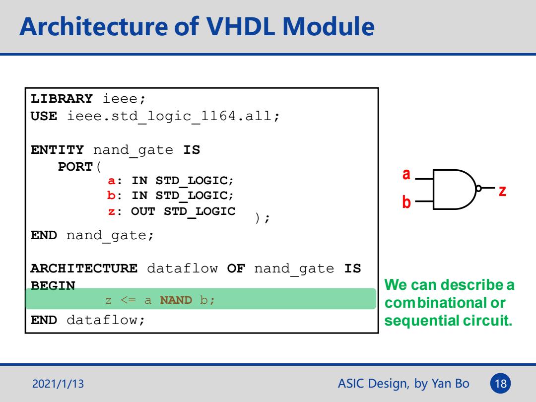
Architecture of VHDL Module LIBRARY ieee; USE ieee.std logic 1164.all; ENTITY nand gate IS PORT( a:IN STD LOGIC; a b:IN STD LOGIC; z:OUT STD LOGIC ) END nand gate; ARCHITECTURE dataflow OF nand gate IS BEGIN We can describe a z<=a NAND b; com binational or END dataflow; sequential circuit. 2021/1/13 ASIC Design,by Yan Bo 18
ASIC Design, by Yan Bo 18 Architecture of VHDL Module LIBRARY ieee; USE ieee.std_logic_1164.all; ENTITY nand_gate IS PORT( ); END nand_gate; ARCHITECTURE dataflow OF nand_gate IS BEGIN END dataflow; a b z 2021/1/13 a: IN STD_LOGIC; b: IN STD_LOGIC; z: OUT STD_LOGIC z <= a NAND b; We can describe a combinational or sequential circuit
Topic2:FPGA Design with Verilog FPGA Design Method Design flow tools Deign Model of Verilog HDL Design style of Verilog HDL Design Examples 。RTL level design Components of Datapath Components of Controller Supplementary 。Synthesizable 。Some experiences 。Other syntax rules 2021/1/13 ASIC Design,by Yan Bo 19
ASIC Design, by Yan Bo Topic2: FPGA Design with Verilog FPGA Design Method Design flow & tools Deign Model of Verilog HDL Design style of Verilog HDL Design Examples • RTL level design • Components of Datapath • Components of Controller Supplementary • Synthesizable • Some experiences • Other syntax rules 2021/1/13 19
Combinational vs.Sequential Combinational Circuit No storage devices The output only depends on the current inputs The most basic component →gates::NAND,NoR The most commonly used modules Decoder/Encoder,MUX/DeMUX,ALU,and so on Parity Check circuit,commonly used in communication system Sequential Circuit - Combinational circuit storage devices The output depends on the current as well as past inputs(STATE) Mealy state machine:the output depends on current input and STATE Moore state machine:the output only depends on the STATE The most basic component →Flip/FIop:DFF The most commonly used modules Register,Counter,and so on Serial Signal Detector,Serial Signal Generator 2021/1/13 ASIC Design,by Yan Bo 20
ASIC Design, by Yan Bo 20 Combinational vs. Sequential • Combinational Circuit – No storage devices The output only depends on the current inputs – The most basic component gates: NAND, NOR – The most commonly used modules Decoder/Encoder, MUX/DeMUX, ALU, and so on Parity Check circuit, commonly used in communication system • Sequential Circuit – Combinational circuit + storage devices The output depends on the current as well as past inputs(STATE) Mealy state machine: the output depends on current input and STATE Moore state machine: the output only depends on the STATE – The most basic component Flip/Flop: DFF – The most commonly used modules Register, Counter, and so on Serial Signal Detector, Serial Signal Generator 2021/1/13
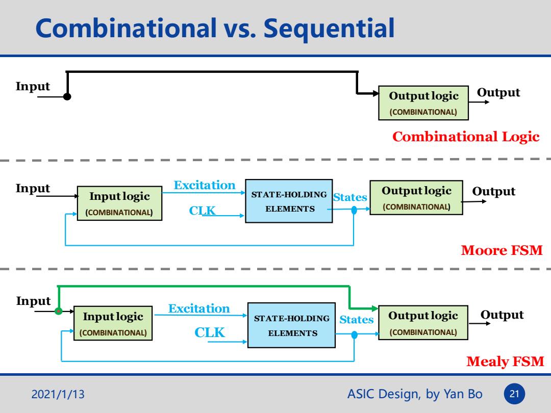
Combinational vs.Sequential Input Outputlogic Output (COMBINATIONAL) Combinational Logic Input Excitation Inputlogic STATE-HOLDING States Output logic Output CLK ELEMENTS (COMBINATIONAL) (COMBINATIONAL) Moore FSM Input Excitation Inputlogic STATE-HOLDING States Outputlogic Output (COMBINATIONAL) CLK ELEMENTS (COMBINATIONAL) Mealy FSM 2021/1/13 ASIC Design,by Yan Bo 21
ASIC Design, by Yan Bo Input logic (COMBINATIONAL) Output logic (COMBINATIONAL) Output STATE-HOLDING ELEMENTS Input States Output logic (COMBINATIONAL) Output Input Input logic (COMBINATIONAL) Output logic (COMBINATIONAL) Output CLK Input States 2021/1/13 21 Mealy FSM Moore FSM Combinational vs. Sequential CLK Combinational Logic Excitation Excitation STATE-HOLDING ELEMENTS
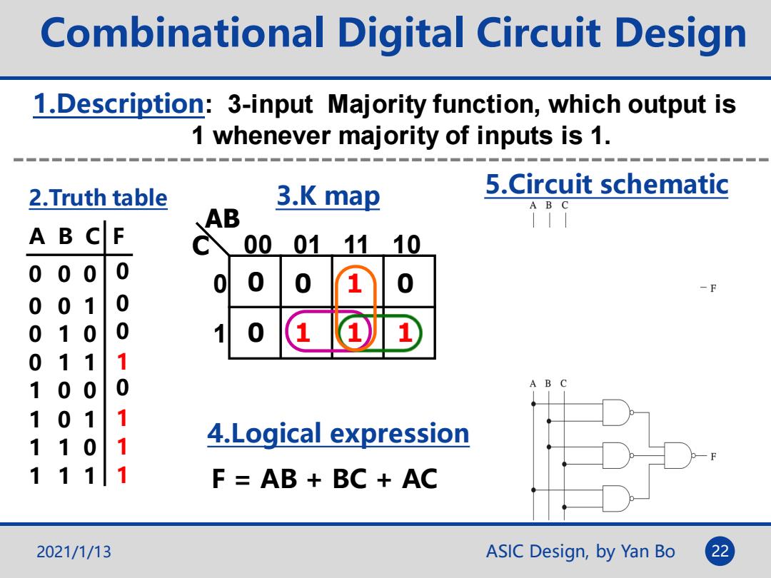
Combinational Digital Circuit Design 1.Description:3-input Majority function,which output is 1 whenever majority of inputs is 1. 2.Truth table 3.K map 5.Circuit schematic A B C AB 11 A B 0001 1110 0 0 -F 0 0 1 0 0 0 0 1 0 1 1 0 0 ABC 1 1 1 0 1 4.Logical expression 1 1 1 1 1 F=AB+BC AC 2021/1/13 ASIC Design,by Yan Bo 22
ASIC Design, by Yan Bo Combinational Digital Circuit Design 2.Truth table A B C F 0 0 0 0 0 1 0 1 0 0 1 1 1 0 0 1 0 1 1 1 0 1 1 1 1.Description: 3-input Majority function, which output is 1 whenever majority of inputs is 1. 1 1 1 1 0 0 0 0 0 C AB 00 01 11 10 0 1 3.K map 0 0 1 0 1 1 1 4.Logical expression F = AB + BC + AC 5.Circuit schematic 2021/1/13 22