
Transmission Electron Microscope Dual Character of Electron particle wave- de Broglie Wavelength 负高压一一 A=h/mv=h/(2meU)i2 2(nm)=1.225/[U(V)]2 0.0037 100,000 0.0025 200,000 Aclectron/AoM=10-5 → 4=0.2nm: 选区光 中可修 Electromagnetic Lens 遂镜 Lorentz force in magnetic field Deflection (Refraction) 变光屏成属相底片 →Focusing&Imaging TEM OM
Transmission Electron Microscope • Dual Character of Electron - particle & wave - de Broglie Wavelength = h / m = h / (2meU) 1/2 (nm) = 1.225 / [U (V)]1/2 0.0037 100,000 0.0025 200,000 electron / OM = 10-5 d0 = 0.2 nm !!! • Electromagnetic Lens Lorentz force in magnetic field Deflection (Refraction) Focusing & Imaging TEM OM
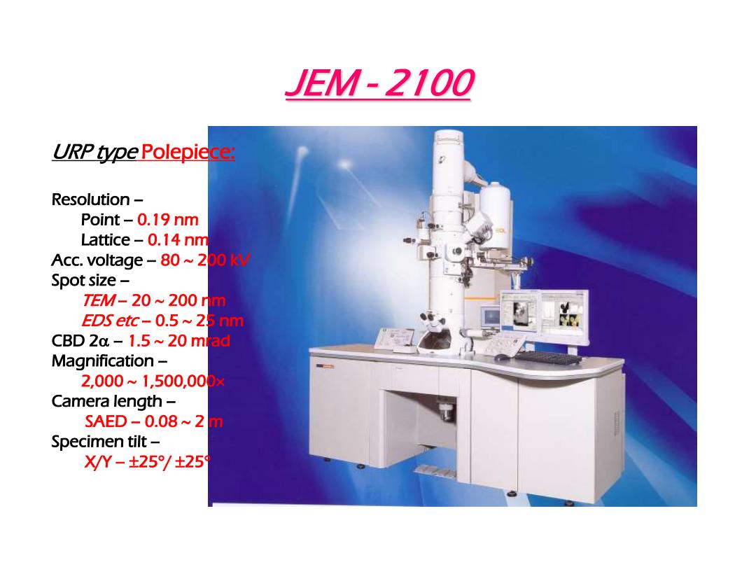
JEM-2100 URP type Polepiece Resolution Point-0.19 nm Lattice-0.14 nm Acc.voltage-80~200 Spot size- TEM-20~200 rm EDS etc-0.5~25m CBD 2a-1.5~20 miad Magnification- 2,000~1,500,000× Camera length- SAED-0.08~2m Specimen tilt- XN-±25/±25
JEM - 2100 URP type Polepiece: Resolution – Point – 0.19 nm Lattice – 0.14 nm Acc. voltage – 80 200 kV Spot size – TEM – 20 200 nm EDS etc – 0.5 25 nm CBD 2 – 1.5 20 mrad Magnification – 2,000 1,500,000 Camera length – SAED – 0.08 2 m Specimen tilt – X/Y – 25/ 25
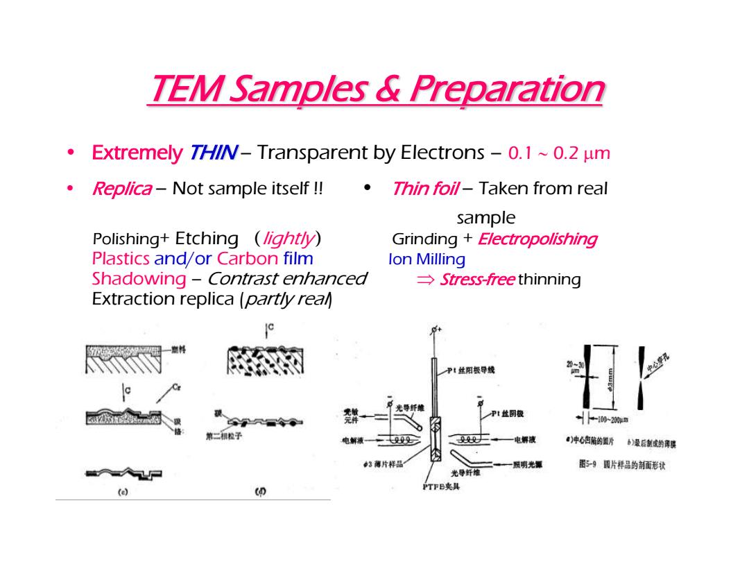
TEM Samples Preparation Extremely TH/N-Transparent by Electrons -0.1 ~0.2 um .Replica-Not sample itself ! Thin foi/-Taken from real sample Polishing+Etching (light/y) Grinding Electropolishing Plastics and/or Carbon film lon Milling Shadowing-Contrast enhanced →Stress-free thinning Extraction replica (partly real P:丝阳根导线 PI丝阴授 1020m 第二和松子 电解液一七一 一电解 ·)冲6由陷的盟片b漫后敏或的阔婆 ◆3薄片样品 一照明光渠 图-9围片样品的制面彩状 光导纤馆 d Q PTFB央具
TEM Samples & Preparation • Extremely THIN – Transparent by Electrons – 0.1 0.2 m • Replica – Not sample itself !! • Thin foil – Taken from real sample Polishing+ Etching (lightly) Grinding + Electropolishing Plastics and/or Carbon film Ion Milling Shadowing – Contrast enhanced Stress-free thinning Extraction replica (partly real)
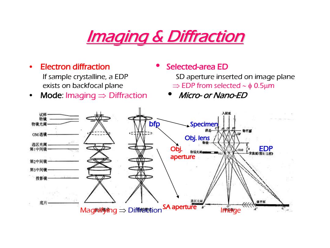
Imaging Diffraction Electron diffraction ●Selected-area ED If sample crystalline,a EDP SD aperture inserted on image plane exists on backfocal plane →EDP from selected~Φ0.5um ·Mode:Imaging→Diffraction ●Micro-or Nano-ED 试样 入京 物镜 物镜光闲 bfp Specimen 样品S OM透镜 7不A20 Obj.lens 选区光阑 第1中间镜 O可 000 EDP 工背雀面(窗能花 aperture 第2中何镜 第3中间镜- 投影镜 底片 装区光彻 Mag*糊mg→Dii他tion SA aperture一 I作ge
Imaging & Diffraction • Electron diffraction • Selected-area ED If sample crystalline, a EDP SD aperture inserted on image plane exists on backfocal plane EDP from selected 0.5m • Mode: Imaging Diffraction • Micro- or Nano-ED bfp SA aperture Obj. aperture Specimen EDP Obj. lens Magnifying Diffraction Image
TEM Contrast Mechanisms .Mass-thickness contrast For replicas-Resolution not so high,limited by that of replica: 2~20nm ·Diffraction contrast For crystalline foil Resolution high,limited by EM:0.2 nm! Two-beam Condition -A centra/bean A strongest diffracted beam Operating reflection - Bright Dark field(BF/DF/CDF)imaging Contrast closely depends on crystal structure and orientation of the sample 。Phase contrast -For very thin crystalline foil multi-beam imaging Resolution very high (High resolution TEM-HRTEM)!! - Contrast closely depends on crystal structure and orientation of the sample Atom resolution TEM(ARTEM attainable !!
TEM Contrast Mechanisms • Mass-thickness contrast – For replicas – Resolution not so high, limited by that of replica: 2 20 nm • Diffraction contrast – For crystalline foil Resolution high, limited by EM: 0.2 nm! – Two-beam Condition – A central bean + A strongest diffracted beam Operating reflection – Bright & Dark field (BF/DF/CDF) imaging – Contrast closely depends on crystal structure and orientation of the sample • Phase contrast – For very thin crystalline foil + multi-beam imaging Resolution very high (High resolution TEM – HRTEM) !! – Contrast closely depends on crystal structure and orientation of the sample – Atom resolution TEM (ARTEM) attainable !!!