Some experiences >Balance architecture Share resources Gated signal >Assignment statement Accident Intentional Latch 2021/1/13 ASIC Design,by Yan Bo 13
ASIC Design, by Yan Bo Some experiences 2021/1/13 13 ➢ Balance architecture ➢ Share resources ➢ Gated signal ➢Assignment statement ➢ Accident / Intentional Latch
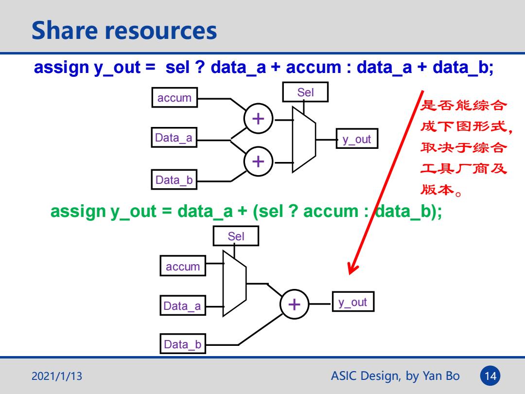
Share resources assign y_out sel data_a+accum data_a data_b; accum Sel 是否能综合 成下图形式, Data a y_out 取决于综合 工具厂商及 Data b 版本。 assign y_out data_a+(sel accum data_b); Sel accum Data a y out Data b 2021/1/13 ASIC Design,by Yan Bo 14
ASIC Design, by Yan Bo Share resources 2021/1/13 14 assign y_out = sel ? data_a + accum : data_a + data_b; assign y_out = data_a + (sel ? accum : data_b); 是否能综合 成下图形式, 取决于综合 工具厂商及 版本。 + Data_a accum y_out + Data_b Sel Data_a + accum y_out Data_b Sel

Share resources (Cont.) module test(rst,clk,updn,q); +1 clk rst inputrst,clk,updn; output [7:0]q; reg[7:0]q; always@(posedge clk or negedge rst) q begin Registers if (!rst)q<=0; else if (updn)q<=q+1; else q<=q-1; end endmodule module test(rst,clk,updn,q); inputrst,clk,updn; clk rst output [7:0]q; reg [7:0]q; integer dir; always@(posedge clk or negedge rst) Registers q if (Irst) q<=0; else q<=q+dir; always @(updn) if (updn)dir=1; else dir =-1; endmodule 2021/1/13 ASIC Design,by Yan Bo 15
ASIC Design, by Yan Bo Share resources (Cont.) 2021/1/13 15 module test(rst, clk, updn, q); input rst, clk, updn; output [7:0] q; reg [7:0] q; always@(posedge clk or negedge rst) begin if (!rst) q<=0; else if (updn) q<=q+1; else q<=q-1; end endmodule + Registers +1 -1 q clk rst + module test(rst, clk, updn, q); input rst, clk, updn; output [7:0] q; reg [7:0] q; integer dir; always@(posedge clk or negedge rst) if (!rst) q<=0; else q<=q+dir; always @ (updn) if (updn) dir = 1; else dir = -1; endmodule + Registers q clk rst +1 -1
Some experiences >Balance architecture Share resources >Gated signal >Assignment statement Accident Intentional Latch 2021/1/13 ASIC Design,by Yan Bo 16
ASIC Design, by Yan Bo Some experiences 2021/1/13 16 ➢ Balance architecture ➢ Share resources ➢ Gated signal ➢Assignment statement ➢ Accident / Intentional Latch
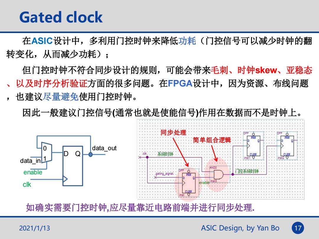
Gated clock 在ASIC设计中,多利用门控时钟来降低功耗(门控信号可以减少时钟的翻 转变化,从而减少功耗) 但门控时钟不符合同步设计的规则,可能会带来毛刺、时钟skw、亚稳态 、以及时序分析验证方面的很多问题。在FPGA设计中,因为资源、布线问题 也建议尽量避免使用门控时钟。 因此一般建议门控信号(通常也就是使能信号)作用在数据而不是时钟上。 同步处理 简单组合逻辑 data_out 系钟 data_inl enable gating_signal clk 如确实需要门控时钟,应尽量靠近电路前端并进行同步处理. 2021/1/13 ASIC Design,by Yan Bo
ASIC Design, by Yan Bo Gated clock 在ASIC设计中,多利用门控时钟来降低功耗(门控信号可以减少时钟的翻 转变化,从而减少功耗); 但门控时钟不符合同步设计的规则,可能会带来毛刺、时钟skew、亚稳态 、以及时序分析验证方面的很多问题。在FPGA设计中,因为资源、布线问题 ,也建议尽量避免使用门控时钟。 因此一般建议门控信号(通常也就是使能信号)作用在数据而不是时钟上。 2021/1/13 17 1 0 data_out data_in enable clk D Q 简单组合逻辑 同步处理 如确实需要门控时钟,应尽量靠近电路前端并进行同步处理