
PN Junctions Biasing a PN Junction Suppose apply a voltage to the PN Junction electrons holes BIAS .Positive terminal of VBIAs attracts electrons Negative terminal of VBIAs attracts holes ⊕ ⊕ ⊕ Makes space charge region bigger ⊕⊕ Increases E field across junction ⊕ Reduces ability of current to flow across junction Bulk P-Type Bulk N-Type →Reverse Bias Now suppose we reverse the polarity of VeIAs holes VBIAS electrons .Positive terminal of VeIAs adds holes to P region .Negative terminal of VBIAs adds electrons to N Makes space charge region smaller ⊕⊕ Decreases E field across junction ⊕ ⊕⊕ ◆ Enhances ability of current to flow across junction →Majority Carrier: Bulk P-Type Bulk N-Type Holes recombine with ionized acceptors Electrons recombine with ionized donors Basic Electronics-Special Lecture for TIPP 2011 11 Gary Drake,Argonne National Lab-Session 3
Basic Electronics – Special Lecture for TIPP 2011 11 Gary Drake, Argonne National Lab – Session 3 PN Junctions Biasing a PN Junction • Suppose apply a voltage to the PN Junction • Now suppose we reverse the polarity of VBIAS VBIAS Positive terminal of VBIAS attracts electrons Negative terminal of VBIAS attracts holes Makes space charge region bigger Increases E field across junction Reduces ability of current to flow across junction Bulk P-Type Bulk N-Type Reverse Bias VBIAS Positive terminal of VBIAS adds holes to P region Negative terminal of VBIAS adds electrons to N Makes space charge region smaller Decreases E field across junction Enhances ability of current to flow across junction Majority Carrier: Holes recombine with ionized acceptors Electrons recombine with ionized donors Bulk P-Type Bulk N-Type electrons holes holes electrons

PN Junctions Biasing a PN Junction (Continued) At a critical bias,space charge region disappears holes electrons Built-in E field across junction is gone Now charge carriers provided by VBIAs can move across PN junction ⊕ ⊕⊕ ⊕ ⊕ 田⊕田 →Forward Bias→Conduction ⊕⊕ ⊕ Each new electron/hole pair pushes existing pair out of bulk Bulk P-Type Bulk N-Type How much voltage is required to reach forward bias? Answer:Related to how much energy is required to remove bound electrons (or holes)from their nuclei →Vork Function Depends on doping concentrations Depends on intrinsic carrier concentration Depends on temperature φ=kT/qln[NaNa/n2] Basic Electronics-Special Lecture for TIPP 2011 12 Gary Drake,Argonne National Lab-Session 3
Basic Electronics – Special Lecture for TIPP 2011 12 Gary Drake, Argonne National Lab – Session 3 PN Junctions Biasing a PN Junction (Continued) • At a critical bias, space charge region disappears • How much voltage is required to reach forward bias? Answer: Related to how much energy is required to remove bound electrons (or holes) from their nuclei Work Function – Depends on doping concentrations – Depends on intrinsic carrier concentration – Depends on temperature VBIAS Built-in E field across junction is gone Now charge carriers provided by VBIAS can move across PN junction Forward Bias Conduction Each new electron/hole pair pushes existing pair out of bulk holes electrons Bulk P-Type Bulk N-Type = kT/q ln [ Nd Na / ni2 ]

Diodes Physical Description Essentially a simple PN Junction ·Symbol IpIODE VDIODE +VDIODE ⊕田田 ⊕ anode cathode 田⊕田 ⊕ ⊕⊕ Bulk P-Type IDIODE Bulk N-Type ■IV Characteristics Shockley Diode Equation Where:Is=Reverse Saturation Current Ip Is [e-[k VD/(naT)-1] k Boltzman Constant (1.38E-23 J/K) T=Temperature Kelvin) q=charge (1.6E-19 C/e-) n=quality factor,1≥n≥2 Vr=k T/q=25.8 mV room temp Thermal Voltage Nonlinear IV relationship In most diodes,Isis very small Basic Electronics-Special Lecture for TIPP 2011 13 Gary Drake,Argonne National Lab-Session 3
Basic Electronics – Special Lecture for TIPP 2011 13 Gary Drake, Argonne National Lab – Session 3 Diodes Physical Description • Essentially a simple PN Junction IV Characteristics • Shockley Diode Equation Where: IS = Reverse Saturation Current k = Boltzman Constant (1.38E-23 J/K) T = Temperature (o Kelvin) q = charge (1.6E19 C/e ) n = quality factor, 1 P n P 2 ID = IS [ ek VD/ (n q T) – 1 ] VDIODE Bulk P-Type Bulk N-Type • Symbol IDIODE VDIODE IDIODE anode cathode ID IS VD VT = k T / q = 25.8 mV @ room temp = Thermal Voltage Nonlinear IV relationship In most diodes, IS is very small
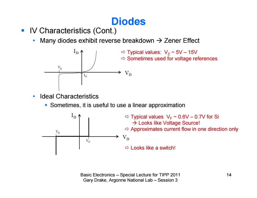
Diodes IV Characteristics (Cont.) Many diodes exhibit reverse breakdown Zener Effect Typical values:V~5V -15V Sometimes used for voltage references VD Ideal Characteristics Sometimes,it is useful to use a linear approximation Typical values V ~0.6V-0.7V for Si Looks like Voltage Source! Approximates current flow in one direction only Vp →Looks like a switch! Basic Electronics-Special Lecture for TIPP 2011 14 Gary Drake,Argonne National Lab-Session 3
Basic Electronics – Special Lecture for TIPP 2011 14 Gary Drake, Argonne National Lab – Session 3 Diodes IV Characteristics (Cont.) • Many diodes exhibit reverse breakdown Zener Effect • Ideal Characteristics Sometimes, it is useful to use a linear approximation ID IS VD VZ Typical values: VZ ~ 5V – 15V Sometimes used for voltage references ID VD VZ VF Typical values VF ~ 0.6V – 0.7V for Si Looks like Voltage Source! Approximates current flow in one direction only Looks like a switch!
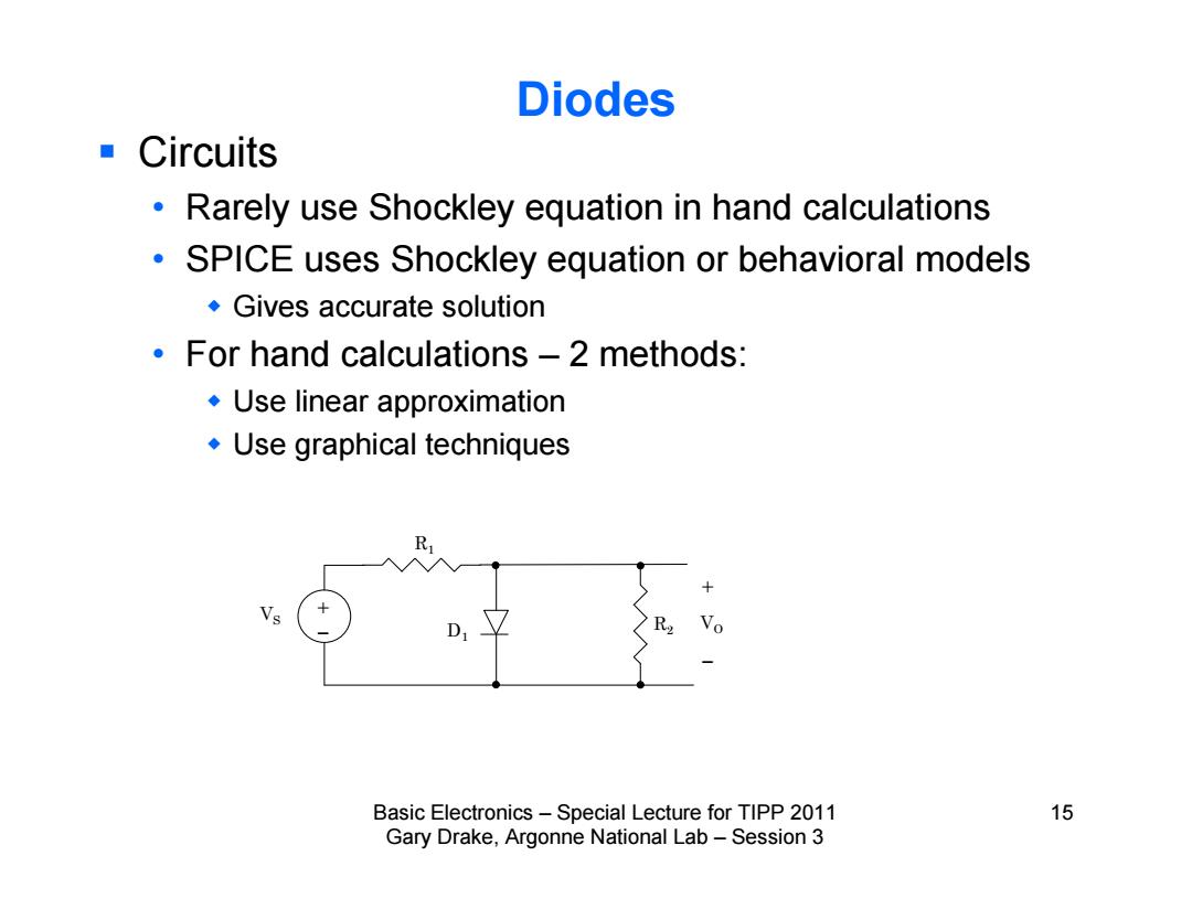
Diodes ■Circuits Rarely use Shockley equation in hand calculations SPICE uses Shockley equation or behavioral models Gives accurate solution For hand calculations -2 methods: .Use linear approximation Use graphical techniques Vs Basic Electronics-Special Lecture for TIPP 2011 15 Gary Drake,Argonne National Lab-Session 3
Basic Electronics – Special Lecture for TIPP 2011 15 Gary Drake, Argonne National Lab – Session 3 Diodes Circuits • Rarely use Shockley equation in hand calculations • SPICE uses Shockley equation or behavioral models Gives accurate solution • For hand calculations – 2 methods: Use linear approximation Use graphical techniques R1 VS D R2 1 VO