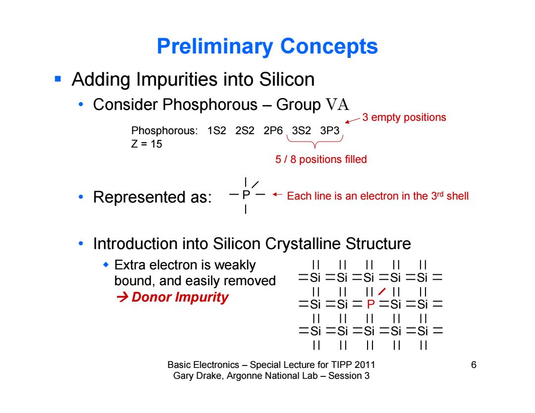
Preliminary Concepts Adding Impurities into Silicon Consider Phosphorous Group VA k一3 empty positions Phosphorous:1S2 2S2 2P6 3S2 3P3 Z=15 5/8 positions filled 1/ Represented as:-P-+Each line is an electron in the 3rd shell Introduction into Silicon Crystalline Structure Extra electron is weakly 川川川I川川 bound,and easily removed 二Si=Si二Si二Si二Si= →Donor Impurity 川川川/川IH =Si二Si=P二Si二Si= 川川川川 二Si二Si二Si二Si二Si= H川 Basic Electronics-Special Lecture for TIPP 2011 6 Gary Drake,Argonne National Lab-Session 3
Basic Electronics – Special Lecture for TIPP 2011 6 Gary Drake, Argonne National Lab – Session 3 Preliminary Concepts Adding Impurities into Silicon • Consider Phosphorous – Group VA • Represented as: • Introduction into Silicon Crystalline Structure Extra electron is weakly bound, and easily removed Donor Impurity Phosphorous: 1S2 2S2 2P6 3S2 3P3 Z = 15 Each line is an electron in the 3rd shell 5 / 8 positions filled Si Si Si Si Si Si Si P Si Si Si Si Si Si Si P 3 empty positions
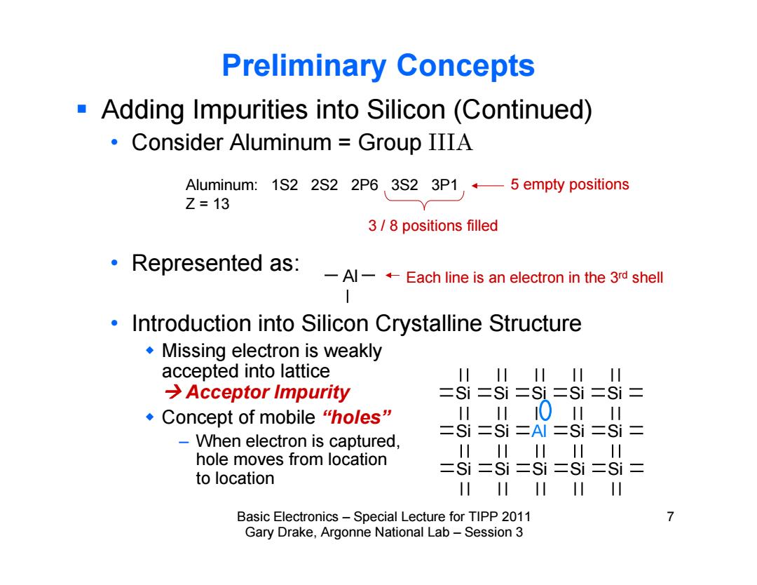
Preliminary Concepts Adding Impurities into Silicon(Continued) Consider Aluminum Group IIIA Aluminum:1S2 2S2 2P6 3S2 3P15 empty positions Z=13 3/8 positions filled Represented as:-Al-Each line is an electron in the 3 shell Introduction into Silicon Crystalline Structure Missing electron is weakly accepted into lattice 川 I川 川 I川 I川 →Acceptor Impurity 二Si二Si=Si=Si二Si= ◆Concept of mobile "holes” 0 川 =Si=Si=Al二Si=Si= -When electron is captured, hole moves from location 川川川川 川 二Si二Si二Si二Si=Si= to location I川 川 Basic Electronics-Special Lecture for TIPP 2011 7 Gary Drake,Argonne National Lab-Session 3
Basic Electronics – Special Lecture for TIPP 2011 7 Gary Drake, Argonne National Lab – Session 3 Preliminary Concepts Adding Impurities into Silicon (Continued) • Consider Aluminum = Group IIIA • Represented as: • Introduction into Silicon Crystalline Structure Missing electron is weakly accepted into lattice Acceptor Impurity Concept of mobile “holes” – When electron is captured, hole moves from location to location Aluminum: 1S2 2S2 2P6 3S2 3P1 Z = 13 Each line is an electron in the 3rd shell 3 / 8 positions filled Si Si Si Si Si Si Si Al Si Si Si Si Si Si Si Al 5 empty positions
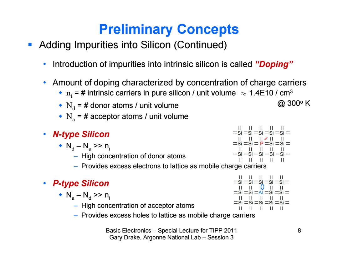
Preliminary Concepts Adding Impurities into Silicon (Continued) Introduction of impurities into intrinsic silicon is called "Doping" Amount of doping characterized by concentration of charge carriers .n;=#intrinsic carriers in pure silicon unit volume1.4E10/cm3 .N=#donor atoms unit volume @300°K .N.=acceptor atoms unit volume 1111川11 ·N-type Silicon =Si=si=si =si=si= 1川1◆川川 ·Na-Na>n si=si=P=Si=si= High concentration of donor atoms =S==8=60=6= 1111111 -Provides excess electrons to lattice as mobile charge carriers 1111川1 ·P-type Silicon =Si=si=si=si=si= 川1川0川日 ·Na-Na>n Si=Si =Al =Si=Si= 111川1 -High concentration of acceptor atoms =Si=si=si=si=si= 1111 -Provides excess holes to lattice as mobile charge carriers Basic Electronics-Special Lecture for TIPP 2011 8 Gary Drake,Argonne National Lab-Session 3
Basic Electronics – Special Lecture for TIPP 2011 8 Gary Drake, Argonne National Lab – Session 3 Preliminary Concepts Adding Impurities into Silicon (Continued) • Introduction of impurities into intrinsic silicon is called “Doping” • Amount of doping characterized by concentration of charge carriers ni = # intrinsic carriers in pure silicon / unit volume y 1.4E10 / cm3 Nd = # donor atoms / unit volume Na = # acceptor atoms / unit volume • N-type Silicon Nd – Na >> ni – High concentration of donor atoms – Provides excess electrons to lattice as mobile charge carriers • P-type Silicon Na – Nd >> ni – High concentration of acceptor atoms – Provides excess holes to lattice as mobile charge carriers @ 300o K
Preliminary Concepts -Adding Impurities into Silicon(Continued) How to make use of mobile charge carriers Bonds can be broken by: Application of an Electric Field Basic principle of how integrated circuits work Application of Light>Photons impart energy >Basic principle of how photo cells work Use reverse principle for light emitting diodes(LEDs) -Heat→Kinetic Energy >Basic use for temperature sensors Generally a bad property for semiconductors... Basic Electronics-Special Lecture for TIPP 2011 9 Gary Drake,Argonne National Lab-Session 3
Basic Electronics – Special Lecture for TIPP 2011 9 Gary Drake, Argonne National Lab – Session 3 Preliminary Concepts Adding Impurities into Silicon (Continued) • How to make use of mobile charge carriers Bonds can be broken by: – Application of an Electric Field » Basic principle of how integrated circuits work – Application of Light Photons impart energy » Basic principle of how photo cells work » Use reverse principle for light emitting diodes (LEDs) – Heat Kinetic Energy » Basic use for temperature sensors » Generally a bad property for semiconductors…
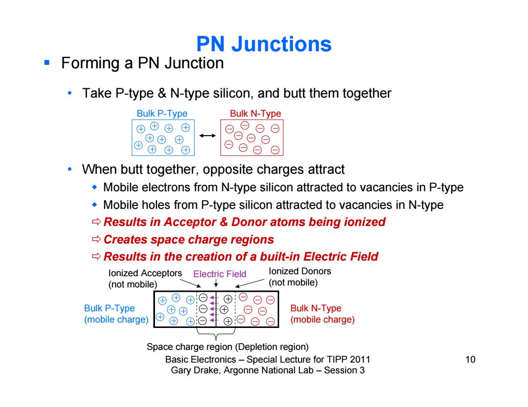
PN Junctions Forming a PN Junction Take P-type N-type silicon,and butt them together Bulk P-Type Bulk N-Type ⊕⊕© ⊕ ⊕⊕⊕ ⊕④田① When butt together,opposite charges attract Mobile electrons from N-type silicon attracted to vacancies in P-type Mobile holes from P-type silicon attracted to vacancies in N-type Results in Acceptor Donor atoms being ionized Creates space charge regions Results in the creation of a built-in Electric Field lonized Acceptors Electric Field lonized Donors (not mobile) (not mobile) ⊕ ©⊙ Bulk P-Type Bulk N-Type (mobile charge) ⊕ ⊕⊙ (mobile charge) Space charge region(Depletion region) Basic Electronics-Special Lecture for TIPP 2011 10 Gary Drake,Argonne National Lab-Session 3
Basic Electronics – Special Lecture for TIPP 2011 10 Gary Drake, Argonne National Lab – Session 3 PN Junctions Forming a PN Junction • Take P-type & N-type silicon, and butt them together • When butt together, opposite charges attract Mobile electrons from N-type silicon attracted to vacancies in P-type Mobile holes from P-type silicon attracted to vacancies in N-type Results in Acceptor & Donor atoms being ionized Creates space charge regions Results in the creation of a built-in Electric Field Bulk P-Type Bulk N-Type Bulk P-Type (mobile charge) Bulk N-Type (mobile charge) Ionized Acceptors (not mobile) Ionized Donors (not mobile) Electric Field Space charge region (Depletion region)