
Diodes Circuits (Continued Example-Use Linear Approximation: If diode is OFF: R Vs D R Ideal: D个 Vo=Vs R2 /R+R2) V: Valid for:Vo Ve Or:Vs<Vg [1+(R/R2) If diode is ON: Ri Vo个 VE Slope [1+(R/R2) Vr[1+(R/R2)] Vo =VE Valid for:I >0 Called a Clamp Circuit Or:Vs>Ve [1+(R1/R2) Basic Electronics-Special Lecture for TIPP 2011 16 Gary Drake,Argonne National Lab-Session 3
Basic Electronics – Special Lecture for TIPP 2011 16 Gary Drake, Argonne National Lab – Session 3 Diodes Circuits (Continued • Example – Use Linear Approximation: I1 R1 VS D R2 1 VO R1 VS VF R2 VO If diode is ON: VO = VF Valid for: I1 > 0 Or: VS > VF [ 1 + (R1 / R2) ] I1 R1 VS R2 VO If diode is OFF: VO = VS R2 / (R1 + R2) Valid for: VO < VF Or: VS < VF [ 1 + ( R1 / R2) ] VO VS VF [ 1 + (R1 / R2) ] Called a Clamp Circuit Ideal: I2 VF Slope [ 1 + (R1 / R2) ]
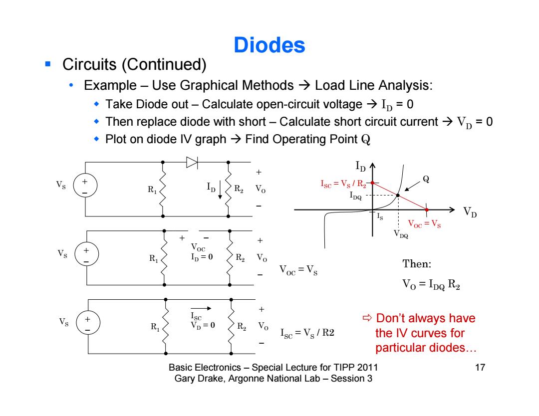
Diodes Circuits (Continued) Example-Use Graphical Methods>Load Line Analysis: Take Diode out-Calculate open-circuit voltage>Ip =0 Then replace diode with short-Calculate short circuit current>Vp=0 ◆Plot on diode IV graph→Find Operating Point Q ID个 Isc Vs R2- Vp Voc=Vs b=0 Voc=Vs Then: Vo=IDQ R2 Vs →Don't always have VD=0 R2 Vo Isc=Vs/R2 the IV curves for particular diodes... Basic Electronics-Special Lecture for TIPP 2011 17 Gary Drake,Argonne National Lab-Session 3
Basic Electronics – Special Lecture for TIPP 2011 17 Gary Drake, Argonne National Lab – Session 3 Diodes Circuits (Continued) • Example – Use Graphical Methods Load Line Analysis: Take Diode out – Calculate open-circuit voltage ID = 0 Then replace diode with short – Calculate short circuit current VD = 0 Plot on diode IV graph Find Operating Point Q ID IS VD R1 VS R2 VO R1 VS R2 VO R1 VS R2 VO VOC ID = 0 VOC = VS ISC = VS / R2 VOC = VS ISC = VS / R2 Q ISC VD = 0 Then: VO = IDQ R2 ID VDQ IDQ Don’t always have the IV curves for particular diodes…

Field Effect Transistors ■Introduction Field Effect Transistors(FETs)are 3-terminal devices,where the current flow between two of the terminals (Drain Source)is controlled through the use of an electric field applied at the third terminal (Gate),which modulates a conduction channel between the two active terminals. Current flow is achieved by drift currents through the channel Charge carriers are majority carriers Drain (p-type holes,n-type electrons) Current flow is uni-directional Gate Several different kinds: Source Metal Oxide Semiconductor FET(MOSFET)+We will focus on this today ◆Junction FET(JFET) Used extensively in HEP Metal Oxide Semiconductor FET(MESFET) Custom ASIC design! High Electron Mobility Transistor (HEMT) Depleted FET(DEPFET) (Many other variations...) Basic Electronics-Special Lecture for TIPP 2011 18 Gary Drake,Argonne National Lab-Session 3
Basic Electronics – Special Lecture for TIPP 2011 18 Gary Drake, Argonne National Lab – Session 3 Introduction • Field Effect Transistors (FETs) are 3-terminal devices, where the current flow between two of the terminals (Drain & Source) is controlled through the use of an electric field applied at the third terminal (Gate), which modulates a conduction channel between the two active terminals. Current flow is achieved by drift currents through the channel Charge carriers are majority carriers (p-type holes, n-type electrons) Current flow is uni-directional • Several different kinds: Metal Oxide Semiconductor FET (MOSFET) Junction FET (JFET) Metal Oxide Semiconductor FET (MESFET) High Electron Mobility Transistor (HEMT) Depleted FET (DEPFET) (Many other variations…) Field Effect Transistors We will focus on this today Gate Source Drain Used extensively in HEP Custom ASIC design!
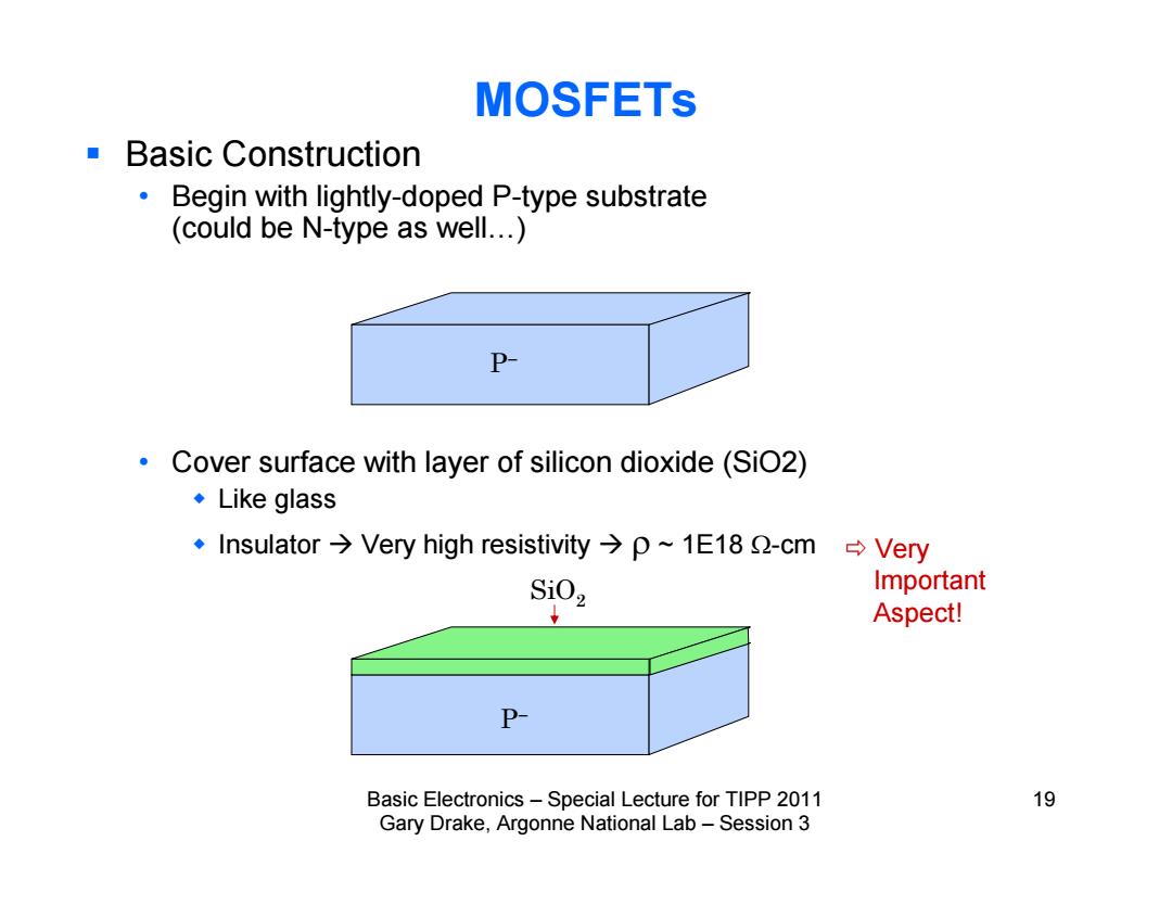
MOSFETs Basic Construction Begin with lightly-doped P-type substrate (could be N-type as well...) P Cover surface with layer of silicon dioxide(SiO2) ◆Like glass ·Insulator→Very high resistivity→p~1E182-cm→Vey SiO2 Important Aspect! P- Basic Electronics-Special Lecture for TIPP 2011 19 Gary Drake,Argonne National Lab-Session 3
Basic Electronics – Special Lecture for TIPP 2011 19 Gary Drake, Argonne National Lab – Session 3 Basic Construction • Begin with lightly-doped P-type substrate (could be N-type as well…) • Cover surface with layer of silicon dioxide (SiO2) Like glass Insulator Very high resistivity ~ 1E18 -cm MOSFETs P P SiO2 Very Important Aspect!
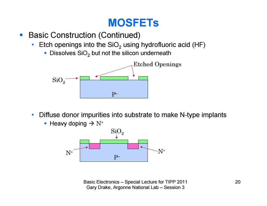
MOSFETs Basic Construction (Continued) Etch openings into the SiO>using hydrofluoric acid(HF) .Dissolves SiO,but not the silicon underneath Etched Openings Si02→ P- Diffuse donor impurities into substrate to make N-type implants ·Heavy doping→Nt SiOz N+ N+ P- Basic Electronics-Special Lecture for TIPP 2011 20 Gary Drake,Argonne National Lab-Session 3
Basic Electronics – Special Lecture for TIPP 2011 20 Gary Drake, Argonne National Lab – Session 3 Basic Construction (Continued) • Etch openings into the SiO2 using hydrofluoric acid (HF) Dissolves SiO2 but not the silicon underneath • Diffuse donor impurities into substrate to make N-type implants Heavy doping N+ MOSFETs P P N N SiO2 SiO2 Etched Openings