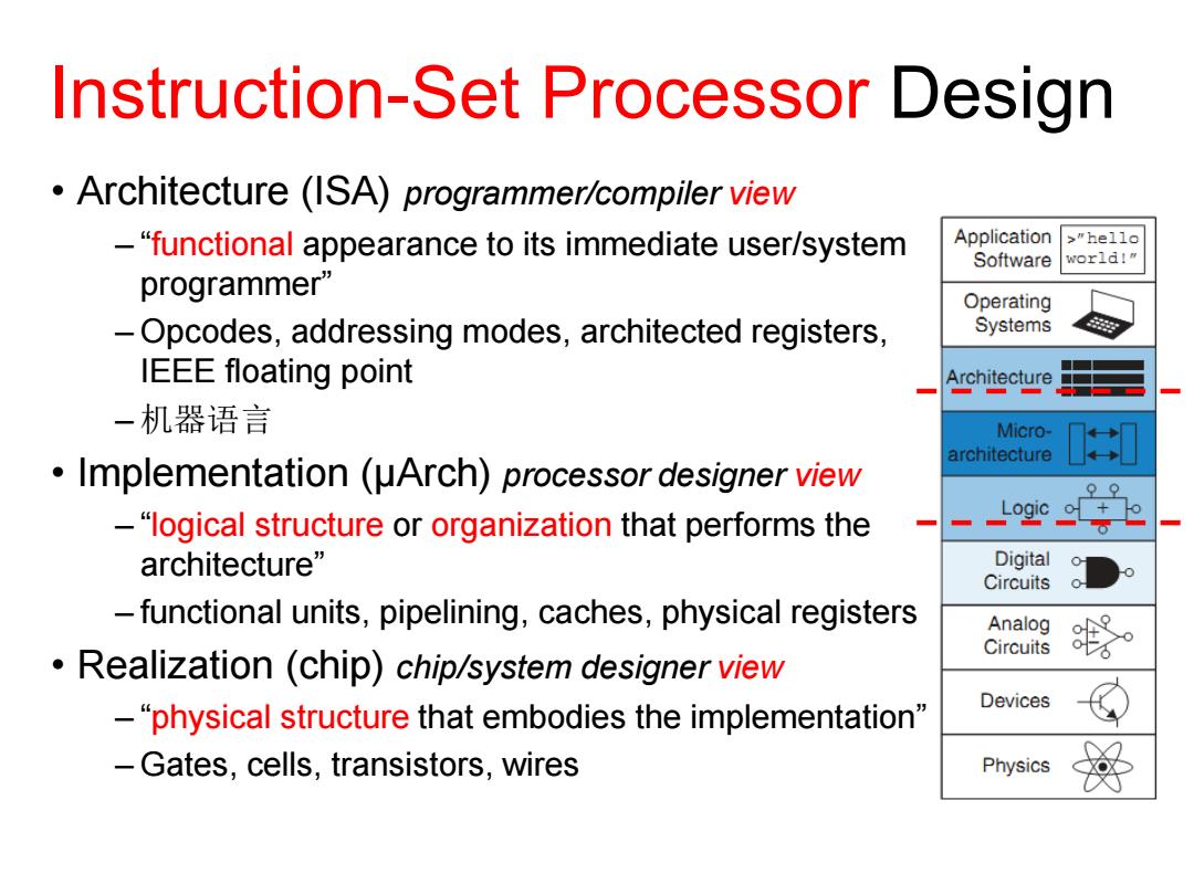
Instruction-Set Processor Design Architecture (ISA)programmer/compiler view -"functional appearance to its immediate user/system Application >"hello Software world!" programmer" Operating -Opcodes,addressing modes,architected registers Systems IEEE floating point Architecture -机器语言 Micro- architecture Implementation (JArch)processor designer view -"logical structure or organization that performs the architecture" Digital Circuits o -functional units,pipelining,caches,physical registers Analog Circuits Realization (chip)chip/system designer view Devices -"physical structure that embodies the implementation' -Gates,cells,transistors,wires Physics
Instruction-Set Processor Design • Architecture (ISA) programmer/compiler view – “functional appearance to its immediate user/system programmer” – Opcodes, addressing modes, architected registers, IEEE floating point – 机器语言 • Implementation (µArch) processor designer view – “logical structure or organization that performs the architecture” – functional units, pipelining, caches, physical registers • Realization (chip) chip/system designer view – “physical structure that embodies the implementation” – Gates, cells, transistors, wires
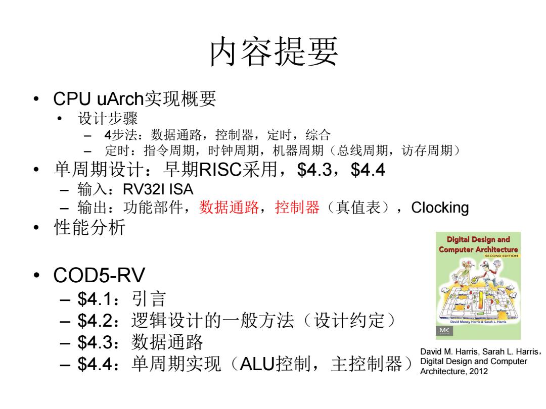
内容提要 ●( CPU uArch实现概要 ·设计步骤 -4步法:数据通路,控制器,定时,综合 定时:指令周期,时钟周期,机器周期(总线周期,访存周期) 。 单周期设计:早期R1SC采用,$4.3,$4.4 -输入:RV32IISA -输出:功能部件,数据通路,控制器(真值表),Clocking ·性能分析 Digital Design and Computer Architecture SECONO EDTION COD5-RV - $4.1:引言 -$4.2:逻辑设计的一般方法(设计约定) M< -$4.3:数据通路 David M.Harris,Sarah L.Harris, $4.4:单周期实现(ALU控制,主控制器) Digital Design and Computer Architecture,2012
内容提要 • CPU uArch实现概要 • 设计步骤 – 4步法:数据通路,控制器,定时,综合 – 定时:指令周期,时钟周期,机器周期(总线周期,访存周期) • 单周期设计:早期RISC采用,$4.3,$4.4 – 输入:RV32I ISA – 输出:功能部件,数据通路,控制器(真值表),Clocking • 性能分析 • COD5-RV – $4.1:引言 – $4.2:逻辑设计的一般方法(设计约定) – $4.3:数据通路 – $4.4:单周期实现(ALU控制,主控制器) David M. Harris, Sarah L. Harris, Digital Design and Computer Architecture, 2012
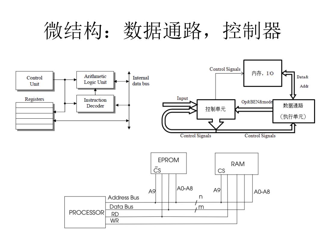
微结构:数据通路,控制器 Control Signals 内存,I0 Control Arithmetic Internal Data& Unit Logic Unit data bus Addr Registers Instruction Input Op&BEN&mode Decoder 控制单元 数据通路 (执行单元) Control Signals Control Signals EPROM RAM Cs CS A9 A0-A8 A9 A0-A8 Address Bus n Data Bus m PROCESSOR RD WR
微结构:数据通路,控制器
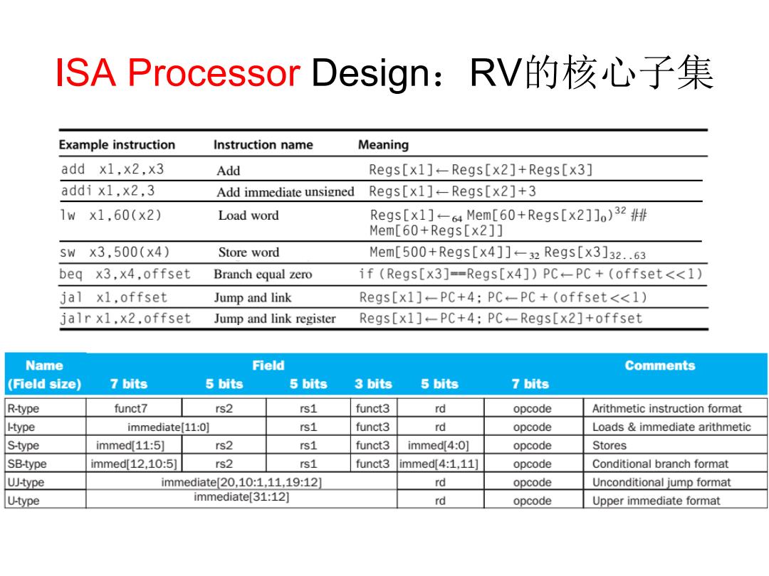
ISA Processor Design:RV的核心子集 Example instruction Instruction name Meaning add x1,x2,x3 Add Regs[x1]-Regs[x2]+Regs[x3] addi x1,x2,3 Add immediate unsigned Regs[x1]-Regs[x2]+3 1wx1,60(x2) Load word Regs[x1]-64 Mem[60+Regs[x2]])32 Mem[60+Regs[x2]] swx3,500(x4) Store word Mem[500+Regs[x4]]-32Regs[x3]32.63 beq x3,x4,offset Branch equal zero if (Regs[x3]--Regs[x4])PC-PC+(offset<<1) jal xl,offset Jump and link Regs[x1]-PC+4;PC-PC+(offset<<1) jalr x1.x2,offset Jump and link register Regs[x1]-PC+4;PC+-Regs[x2]+offset Name Field Comments (Field size) 7 bits 5 bits 5 bits 3 bits 5 bits 7 bits R-type funct7 rs2 rs1 funct3 rd opcode Arithmetic instruction format I-type immediate[11:0] rs1 funct3 rd opcode Loads immediate arithmetic S-type immed[11:5] rs2 rs1 funct3 immed[4:0] opcode Stores SB-type immed[12.10:5] rs2 rs1 funct3 immed[4:1,11] opcode Conditional branch format UJ-type immediate20,10:1,11,19:12] rd opcode Unconditional jump format U-type immediate[31:12] rd opcode Upper immediate format
ISA Processor Design:RV的核心子集

数据通路Abstract/Simplified View RV Instruction Execution Phases Instruction Fetch Data Instruction Decode Regs威er# Address Instruction Registers Address Register Fetch Regster memory Data Register# memory ALU Operations Deta -Optional Memory Operations Optional Register Write back Calculate Next Instruction Address Two types of functional units elements that operate on data values (combinational) elements that contain state (sequential) 6
数据通路Abstract / Simplified View • RV Instruction Execution Phases – Instruction Fetch – Instruction Decode – Register Fetch – ALU Operations – Optional Memory Operations – Optional Register Write back – Calculate Next Instruction Address • Two types of functional units – elements that operate on data values (combinational) – elements that contain state (sequential) 6