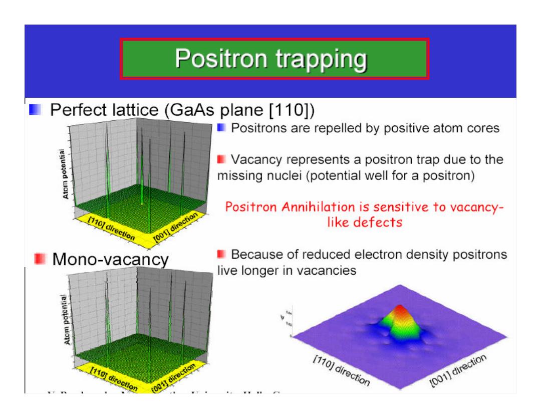
Positron trapping Perfect lattice (GaAs plane [110]) Positrons are repelled by positive atom cores Vacancy represents a positron trap due to the missing nuclei(potential well for a positron) Positron Annihilation is sensitive to vacancy- [110]direction [001]direction like defects Mono-vacancy Because of reduced electron density positrons live longer in vacancies 1110]direction (001 direction [110]direction L001】direction
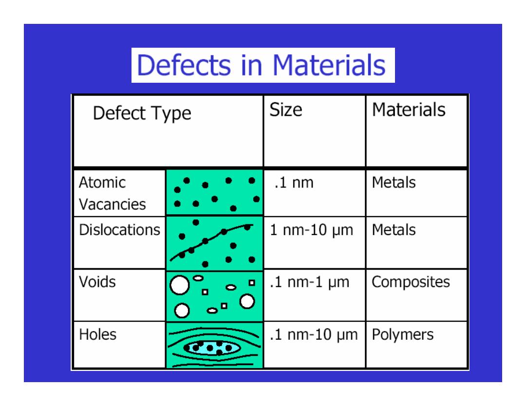
Defects in Materials Defect Type Size Materials Atomic .1nm Metals Vacancies Dislocations 1nm-10μm Metals Voids .1nm-1μm Composites Holes .1nm-10μm Polymers
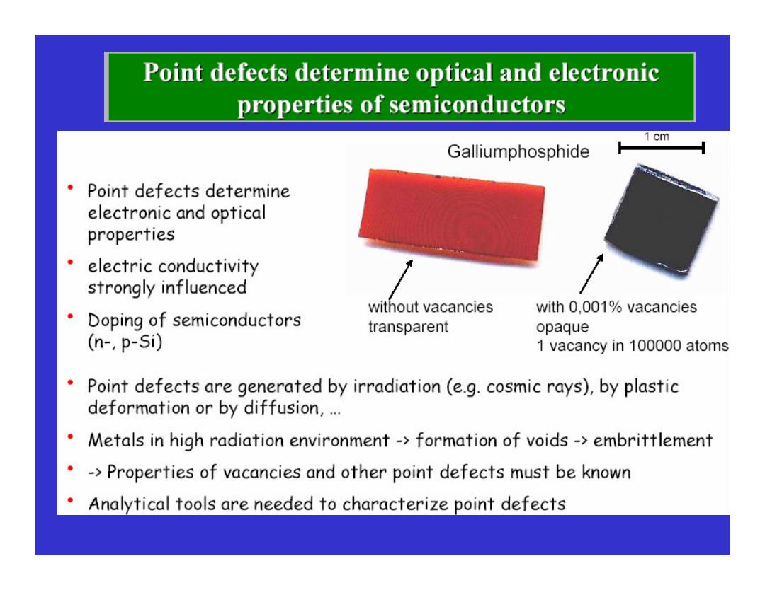
Point defects determine optical and electronic properties of semiconductors 1cm Galliumphosphide Point defects determine electronic and optical properties electric conductivity strongly influenced without vacancies with 0,001%vacancies Doping of semiconductors transparent opaque (n-,p-Si) 1 vacancy in 100000 atoms Point defects are generated by irradiation(e.g.cosmic rays),by plastic deformation or by diffusion,... Metals in high radiation environment->formation of voids->embrittlement .-Properties of vacancies and other point defects must be known Analytical tools are needed to characterize point defects
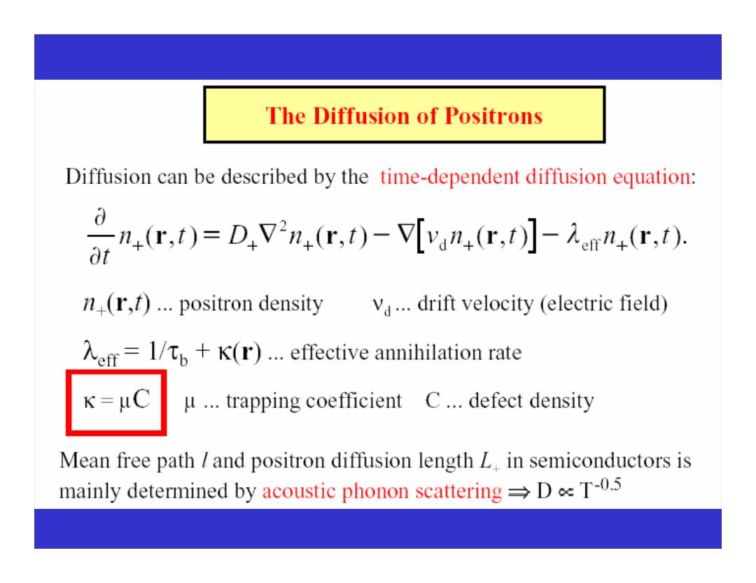
The Diffusion of Positrons Diffusion can be described by the time-dependent diffusion equation: n,1)=D,n4r,)-[n,c,t]-nn,c, ot n(r,t)...positron density Va...drift velocity (electric field) =1/tp+K(r)...effective annihilation rate K=μC u.trapping coefficient C...defect density Mean free path and positron diffusion length L.in semiconductors is mainly determined by acoustic phonon scatteringDT-0.5
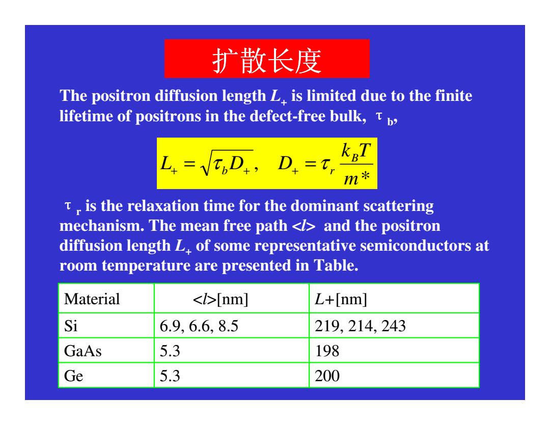
扩散长度 中 The positron diffusion length L.is limited due to the finite lifetime of positrons in the defect-free bulk,T b> L.=,D.,D.= kgT m* t,is the relaxation time for the dominant scattering mechanism.The mean free path <l>and the positron diffusion length L.of some representative semiconductors at room temperature are presented in Table. Material <>[nm] L+[nm] Si 6.9,6.6,8.5 219,214,243 GaAs 5.3 198 Ge 5.3 200
The positron diffusion length L+ is limited due to the finite lifetime of positrons in the defect-free bulk, ?b, ? r is the relaxation time for the dominant scattering mechanism. The mean free path <l> and the positron diffusion length L+ of some representative semiconductors at room temperature are presented in Table. Material <l>[nm] L+[nm] Si 6.9, 6.6, 8.5 219, 214, 243 GaAs 5.3 198 Ge 5.3 200 ᠽᬷ䭓ᑺ * , m k T L D D B b r = τ =τ + + +