PSSD-Topics 1.Basic work such as identification of defects:defect formation, migration,agglomeration and annealing. 2.Momentum distribution studies of defects:coincidence Doppler broadening,angular correlation of annihilation radiation (ACAR) 3.Low-k/High-k dielectric insulating materials in semiconductor devices 4.Theoretical calculations of momentum distributions and positron lifetimes 5.Slow beam studies of surface and near surface regions of semiconductors 6.High resolution positron lifetime studies of semiconductors 7.Semiconductor defects studied by the experimental methods other than positron annihilation 8.Industrial application of positron annihilation to semiconductor devices
PSSD-Topics 1. Basic work such as identification of defects: defect formation, migration, agglomeration and annealing. 2. Momentum distribution studies of defects: coincidence Doppler broadening, angular correlation of annihilation radiation (ACAR). 3. Low-k/High-k dielectric insulating materials in semiconductor devices 4. Theoretical calculations of momentum distributions and positron lifetimes 5. Slow beam studies of surface and near surface regions of semiconductors 6. High resolution positron lifetime studies of semiconductors 7. Semiconductor defects studied by the experimental methods other than positron annihilation 8. Industrial application of positron annihilation to semiconductor devices
Positron Annihilation in Semiconductors Defect Studies R.Krause-Rehberg H.S.Leipner Springer Series in Solid-State Science,1998
Positron Annihilation in Semiconductors Defect Studies R.Krause-Rehberg H.S.Leipner Springer Series in Solid-State Science, 1998
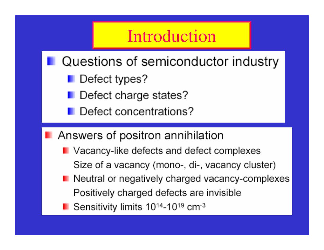
Introduction Questions of semiconductor industry Defect types? Defect charge states? Defect concentrations? Answers of positron annihilation Vacancy-like defects and defect complexes Size of a vacancy (mono-,di-,vacancy cluster) Neutral or negatively charged vacancy-complexes Positively charged defects are invisible Sensitivity limits 1014-1019 cm-3
I n t r o d u c t i o n
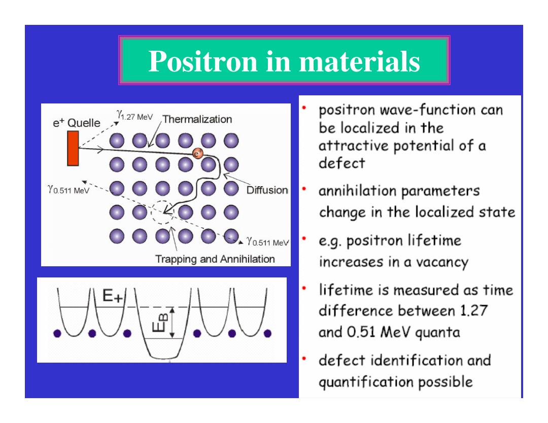
Positron in materials positron wave-function can e+Quelle 11.27 Mev Thermalization be localized in the attractive potential of a defect Diffusion annihilation parameters change in the localized state Y0.511 Mev e.g.positron lifetime Trapping and Annihilation increases in a vacancy 59 lifetime is measured as time difference between 1.27 and 0.51 MeV quanta defect identification and quantification possible
Positron in materials
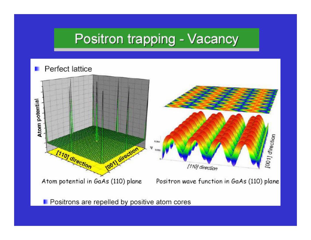
Positron trapping -Vacancy Perfect lattice [110]direction (001]direction (110]direction Atom potential in GaAs(110)plane Positron wave function in GaAs(110)plane Positrons are repelled by positive atom cores