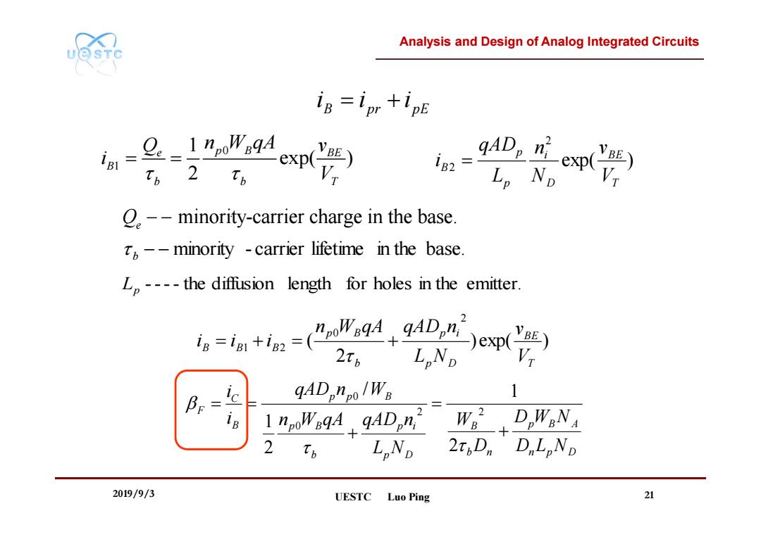
Analysis and Design of Analog Integrated Circuits UOSTC ig=ipr+ipE L。ND O--minority-carrier charge in the base. --minority -carrier lifetime in the base. Lp----the diffusion length for holes in the emitter. 2tp qADpnpo/W8 1 Br= 2 1 npoWqA,qADon W。2,D,WgNA 2 Tp LoNp 2TD DLND 2019/9/3 UESTC Luo Ping 21
Analysis and Design of Analog Integrated Circuits UESTC Luo Ping 2019/9/3 21 0 1 1 exp( ) 2 e p B BE B b b T Q n W qA v i V exp( ) 2 2 T BE D i p p B V v N n L qAD i B pr pE i i i minority - carrier lifetime in the base. b ---- the diffusion length for holes in the emitter. Lp minority-carrier charge in the base. Qe ) exp( ) 2 ( 2 0 1 2 T BE p D p i b p B B B B V v L N n W qA qAD n i i i n p D p B A b n B p D p i b p B p p B B C F D L N D W N D W L N n W qA qAD n qAD n W i i 2 1 2 1 / 2 2 0 0
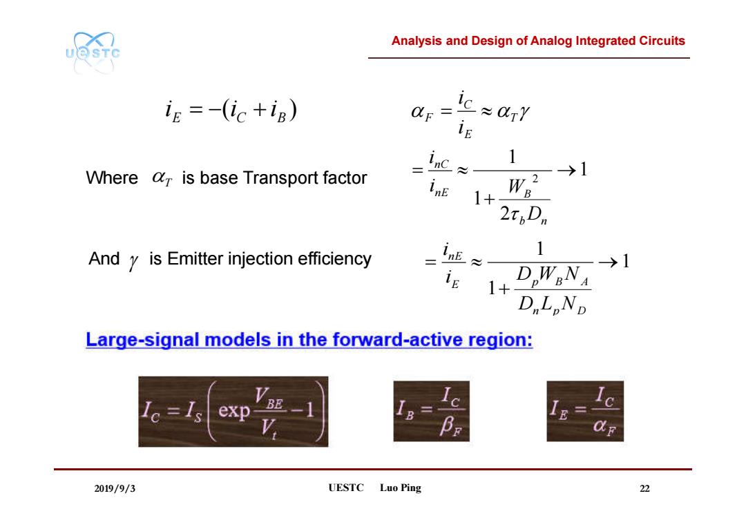
Analysis and Design of Analog Integrated Circuits UQSTC ig =-(ic +iB) ic≈0rY OF- Where 7 is base Transport factor inc 1+ 2→1 2tpDn 1 And y is Emitter injection efficiency in返 iE 1 DWN→] D.LNp Large-signal models in the forward-active region: exp V BE -1 I:- 2019/9/3 UESTC Luo Ping 22
Analysis and Design of Analog Integrated Circuits 2019/9/3 UESTC Luo Ping 22 ( ) E C B i i i T E C F i i T 1 2 1 1 2 b n nE B nC D i W i Where is base Transport factor And is Emitter injection efficiency 1 1 1 n p D E p B A nE D L N i D W N i
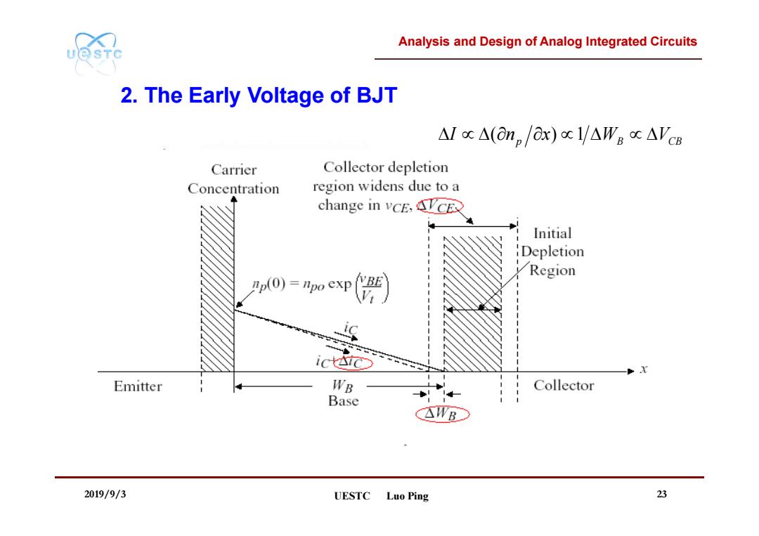
Analysis and Design of Analog Integrated Circuits UQSTC 2.The Early Voltage of BJT △Ioc△(anp/ax)ocl/△WE AVCB Carrier Collector depletion Concentration region widens due to a change in vCE,ACES Initial Depletion Region p(0)=npo exp X Emitter WB Collector Base 个WB 2019/9/3 UESTC Luo Ping 23
Analysis and Design of Analog Integrated Circuits 2019/9/3 UESTC Luo Ping 23 2. The Early Voltage of BJT p WB VCB I (n x) 1

Analysis and Design of Analog Integrated Circuits UQSTC o) 2 Dic=9 =-Ic n OVCE 9.2 OVCE QB OVCE For a uniform base transistor, g =WaN so that the derivative becomes ote-ic ow n OV CE OVCE WE OVCE V 今Va=-wowa Where,D is called the Early voltage Modified large signal VBEA model becomes: VBE3 VBE2 ie=1s(1+ VCE)exp(VI V BE VBEI VCE VA 2019/9/3 UESTC Luo Ping 24
Analysis and Design of Analog Integrated Circuits 2019/9/3 UESTC Luo Ping 24 exp( ) 2 T BE B n i C V v Q qAD n i CE B B C CE B T BE B n i CE C v Q Q I v Q V V Q qAD n v i (exp ) 2 2 QB WBNA B CE A B A C CE B B C CE C W v V W V I v W W I v i VA For a uniform base transistor, so that the derivative becomes Where, is called the Early voltage (1 ) exp( ) T BE A CE C S V v V v i I Modified large signal model becomes:
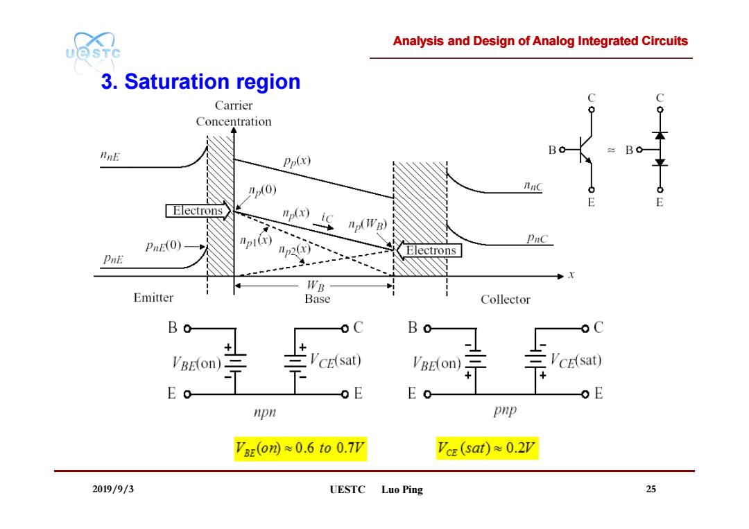
Analysis and Design of Analog Integrated Circuits UQSTC 3.Saturation region C Carrier Concentration InE Bo B Pp(x) np(0) C E E [Electrons npx)ic np(WB) P0) nplr)) PnC Electrons PnE WB- Emitter Base Collector 'BEon)三 三'CE(sat) VcE(sat) o F npn pnp 'z(om≈0.600.7V V'ce(sat)≈0.2V 2019/9/3 UESTC Luo Ping 25
Analysis and Design of Analog Integrated Circuits 2019/9/3 UESTC Luo Ping 25 3. Saturation region