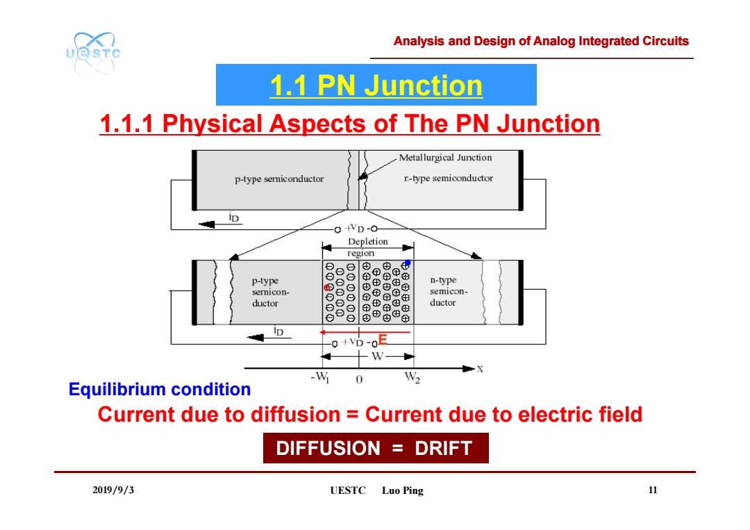
Analysis and Design of Analog Integrated Circuits UQSTC 1.1 PN Junction 1.1.1 Physical Aspects of The PN Junction Metallurgical Junction p-type semiconductor r-type semiconductor 0 4VD-0 Depletion region e p-type 9 的® 的 中 n-type semicon- semicon- ductor e 8 ⊙⊙ ⊕ ductor o & 由 母 D 0+D-o目 W -W 0 W2 Equilibrium condition Current due to diffusion Current due to electric field DIFFUSION DRIFT 2019/9/3 UESTC Luo Ping 11
Analysis and Design of Analog Integrated Circuits 2019/9/3 UESTC Luo Ping 11 1.1.1 Physical Aspects of The PN Junction E Current due to diffusion = Current due to electric field DIFFUSION = DRIFT Equilibrium condition 1.1 PN Junction
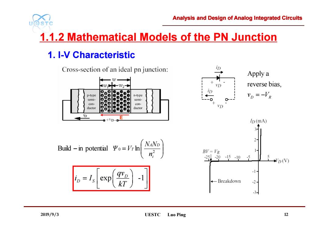
Analysis and Design of Analog Integrated Circuits UQSTC 1.1.2 Mathematical Models of the PN Junction 1.I-V Characteristic Cross-section of an ideal pn junction: D Apply a W1十Ww2 D reverse bias, p-type n-type Vp=-VR 0 semi- con- con- ductor 0 VD ⊙ ductor 0 D o+VD-0 Ip (mA) 2 NAND Build-in potential 平o=Vrh n BV=VR 1 220-5195 D(V) =Is exp -1 kT 4 Breakdown -2 3 2019/9/3 UESTC Luo Ping 12
Analysis and Design of Analog Integrated Circuits 2019/9/3 UESTC Luo Ping 12 1.1.2 Mathematical Models of the PN Junction 2 Build in potential 0 ln i A D T n N N Ψ V Apply a reverse bias, D R v V exp -1 D D S qv i I kT 1. I-V Characteristic E
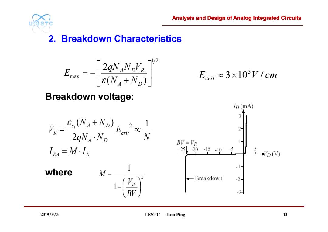
Analysis and Design of Analog Integrated Circuits UOSTC 2.Breakdown Characteristics 7/2 2qN NDVR E(N+Np) Em≈3×10⁵V/cm Breakdown voltage: Ip (mA) R=E NA+ND)E 3 2 2qN4·ND BV=VR IR4=M·IR 2205-95 D(V) 1 -1 where M= +Breakdown -2 BV 3 2019/9/3 UESTC Luo Ping 13
Analysis and Design of Analog Integrated Circuits 2019/9/3 UESTC Luo Ping 13 2. Breakdown Characteristics Breakdown voltage: where 1 2 max 2 ( ) A D R A D qN N V E N N RA R crit A D s A D R I M I N E qN N N N V i 1 2 ( ) 2 n R BV V M 1 1 Ecrit 3 10 V / cm 5
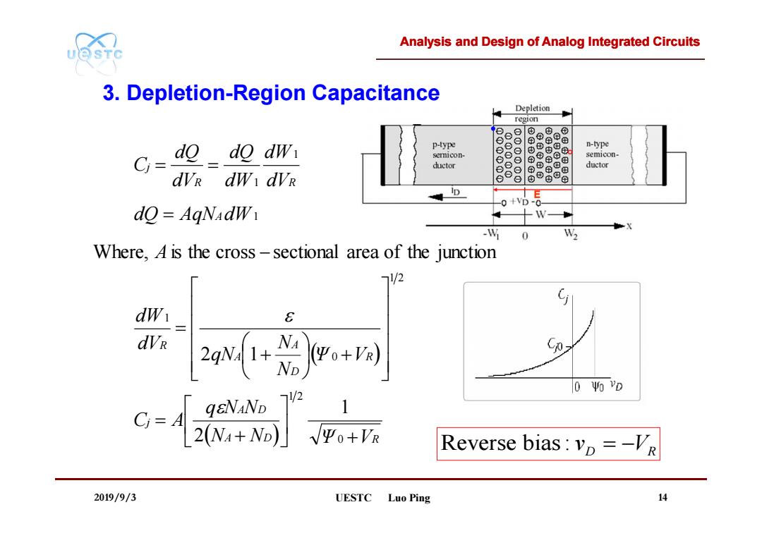
Analysis and Design of Analog Integrated Circuits UQSTC 3.Depletion-Region Capacitance Depletion region 8888 p-type n-type C= dodo dw semicon- ⊙⊙ semicon- ductor ductor dvr dw dvR D e 0+VD- do AgNadW -W 0 W2 Where,A is the cross-sectional area of the junction /2 E dVR 2o+岩+同 0 Yo YD qeNaND C-4 72 2WM+No]Vo+ Reverse bias:vp =-VR 2019/9/3 UESTC Luo Ping 14
Analysis and Design of Analog Integrated Circuits 2019/9/3 UESTC Luo Ping 14 A D R A D j R D A A R A R R j N N Ψ V q N N C A Ψ V N N qN dV dW A dQ AqN dW dV dW dW dQ dV dQ C 0 1 2 1 2 0 1 1 1 1 1 2 2 1 Where, is the cross sectional area of the junction 3. Depletion-Region Capacitance Reverse bias : D R v V
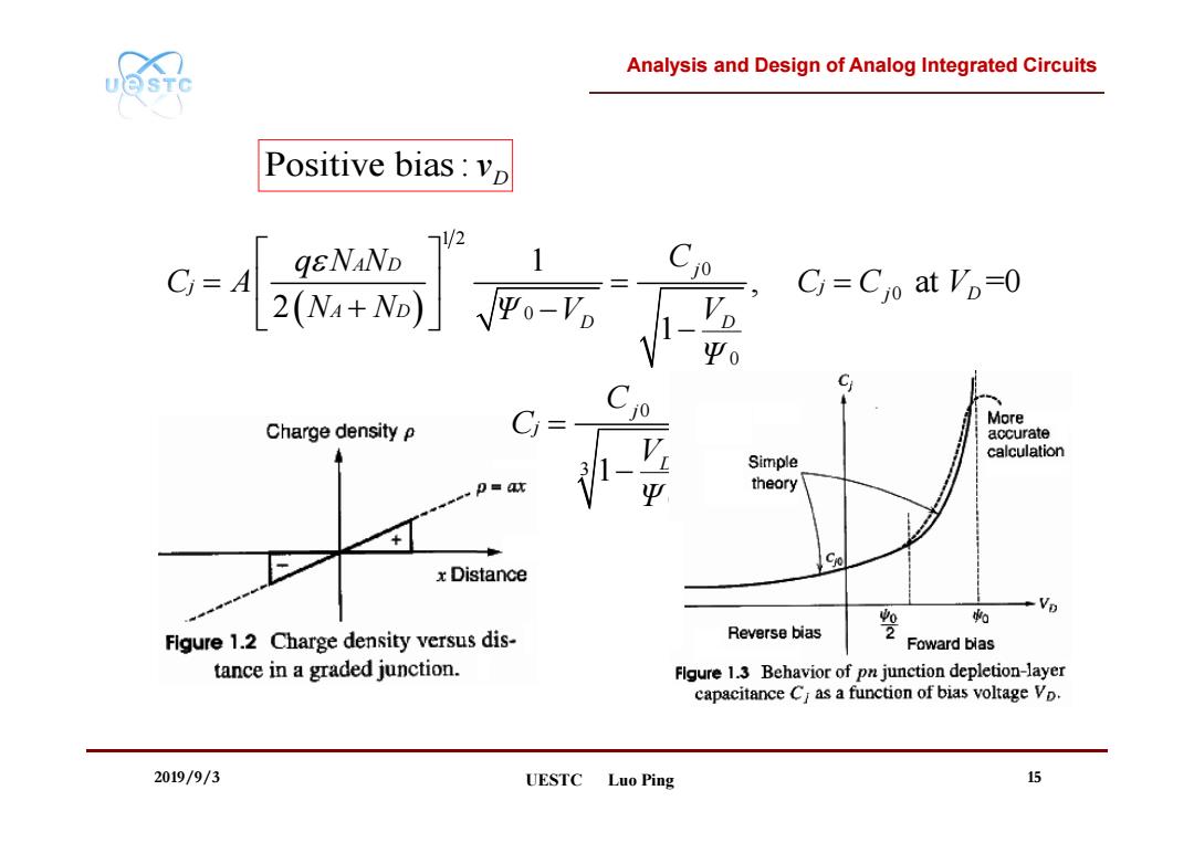
Analysis and Design of Analog Integrated Circuits UQSTC Positive bias:vp C=Cjo at Vp=0 Ψ0 C More Charge density P Ci= accurate Simple calculation p=ax Ψ theory 90 xDistance % Figure 1.2 Charge density versus dis- Reverse bias 2 Foward blas tance in a graded junction. Flgure 1.3 Behavior of pn junction depletion-layer capacitance Ci as a function of bias voltage Vp. 2019/9/3 UESTC Luo Ping 15
Analysis and Design of Analog Integrated Circuits 2019/9/3 UESTC Luo Ping 15 1 2 0 0 0 0 1 , at =0 2 1 A D j j j j D A D D D q N N C C A C C V N N Ψ V V Ψ Positive bias : Dv 0 3 0 1 j j D C C V Ψ