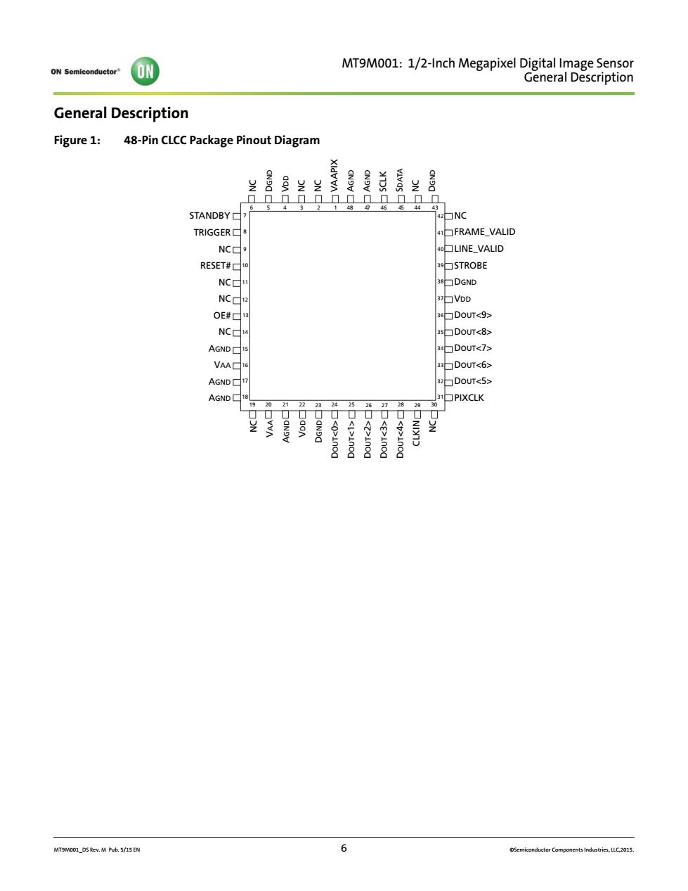
wsasastoO MT9Mo1:1/21nchMegapdD2iagm8eSto General Description Figure 1: 48-Pin CLCC Package Pinout Diagram STANDBY TRIGGERC FRAME VALD ▣LNE_VALID RESET# 9▣STROBE DGND DoUr<9> ▣D0UT<8 AGND DOUT<7> DOUT<6> DOUT<5> AGND M hS EN 6
MT9M001_DS Rev. M Pub. 5/15 EN 6 ©Semiconductor Components Industries, LLC,2015. MT9M001: 1/2-Inch Megapixel Digital Image Sensor General Description General Description Figure 1: 48-Pin CLCC Package Pinout Diagram 6 48 47 46 45 5 4 3 2 1 44 43 19 20 21 22 23 24 25 26 27 28 29 30 7 8 9 10 11 12 13 14 15 16 17 18 42 41 40 39 38 37 36 35 34 33 32 31 STANDBY TRIGGER NC RESET# NC NC OE# NC AGND VAA AGND AGND NC FRAME_VALID LINE_VALID STROBE DGND VDD DOUT<9> DOUT<8> DOUT<7> DOUT<6> DOUT<5> PIXCLK NC VAA AGND VDD DGND DOUT<0> DOUT<1> DOUT<2> DOUT<3> DOUT<4> CLKIN NC NC DGND VDD NC NC VAAPIX AGND AGND SCLK SDATA NC DGND
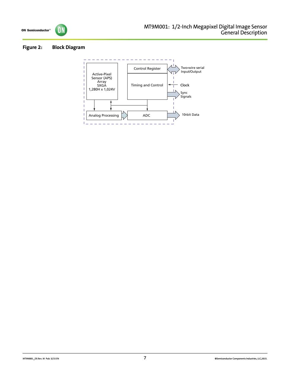
ON MT9M001:1/2-Inch Megapixel Digital Ima 3ea8pt Figure 2: Block Diagram Control Register r (APS) ,280X1024y Timing and Control Analog Processing AD 10-bit Data
MT9M001_DS Rev. M Pub. 5/15 EN 7 ©Semiconductor Components Industries, LLC,2015. MT9M001: 1/2-Inch Megapixel Digital Image Sensor General Description Figure 2: Block Diagram Clock Two-wire serial Input/Output 10-bit Data Sync Signals Control Register Analog Processing Active-Pixel Sensor (APS) Array SXGA 1,280H x 1,024V Timing and Control ADC
O① MT9Mo1:1/21nchMegapdD2iagm8eSto Table3: Pin Descriptions Pin Numbers Symbol Type Description 29 CLKIN Input Clock in.Master clock into sensor(48 MHz maximum). 13 OE# Input 10 RESET# Input Reset.Activates (LW)asynchronous reset of sensor.All registers assume 6 Input clockClock for serial interface. STANDBY Input EtndpytRtgmGWsandboymodedablesanaogbiasccutyfor TRIGGER rigger.Activates(HIGH)snapshot sequence. 45 SDATA tput adata.Serial data bus res 1.5KQ istor to 3.3V fo ull-up 24-28,32-36 ata out D R) 0T9 (MS FRAME VALID data outp during fran me ofv d pix LINE _VAUD Output aeRagdoigr5pmsdHGHdunglimeofseectabievaidpweldhta PIXCLK Output 39 STROBE Output Strobe.Output is pulsed HIGH to indicate sensor reset operation of pixel array has completed. 517247 AGND Supply Anaog ground.Provide isolated ground for ana block and pixel array. 5,23,38,43 Supp igital ground.Provide isolatedground for digital block. 16,20 ock,3.3V+0.3V. VAAPIX Supp吵 nalog pixel power powe upply for 3.3V0.3V3.3 4,22,37 Supply Digital power.Provide power supply for digital block3.3V3V. No connect.These pins must be left unconnected. M hS EN
MT9M001_DS Rev. M Pub. 5/15 EN 8 ©Semiconductor Components Industries, LLC,2015. MT9M001: 1/2-Inch Megapixel Digital Image Sensor General Description Table 3: Pin Descriptions Pin Numbers Symbol Type Description 29 CLKIN Input Clock in. Master clock into sensor (48 MHz maximum). 13 OE# Input Output enable. OE# when HIGH places outputs DOUT<0:9>, FRAME_VALID, LINE_VALID, PIXCLK, and STROBE into a tri-state configuration. 10 RESET# Input Reset. Activates (LOW) asynchronous reset of sensor. All registers assume factory defaults. 46 SCLK Input Serial clock. Clock for serial interface. 7 STANDBY Input Standby. Activates (HIGH) standby mode, disables analog bias circuitry for power saving mode. 8 TRIGGER Input Trigger. Activates (HIGH) snapshot sequence. 45 SDATA Input/Output Serial data. Serial data bus, requires 1.5K resistor to 3.3V for pull-up. 24–28, 32–36 DOUT<0–9> Output Data out. Pixel data output bits 0:9, DOUT<9> (MSB), DOUT<0> (LSB). 41 FRAME_VALID Output Frame valid. Output is pulsed HIGH during frame of valid pixel data. 40 LINE_VALID Output Line valid. Output is pulsed HIGH during line of selectable valid pixel data (see Reg0x20 for options). 31 PIXCLK Output Pixel clock. Pixel data outputs are valid during falling edge of this clock. Frequency = (master clock). 39 STROBE Output Strobe. Output is pulsed HIGH to indicate sensor reset operation of pixel array has completed. 15,17,18,21, 47, 48 AGND Supply Analog ground. Provide isolated ground for analog block and pixel array. 5, 23, 38, 43 DGND Supply Digital ground. Provide isolated ground for digital block. 16, 20 VAA Supply Analog power. Provide power supply for analog block, 3.3V ±0.3V. 1 VAAPIX Supply Analog pixel power. Provide power supply for pixel array, 3.3V ±0.3V (3.3V). 4, 22, 37 VDD Supply Digital power. Provide power supply for digital block, 3.3V ±0.3V. 2, 3 ,6, 9, 11, 12,14, 19, 30, 42, 44 NC — No connect. These pins must be left unconnected
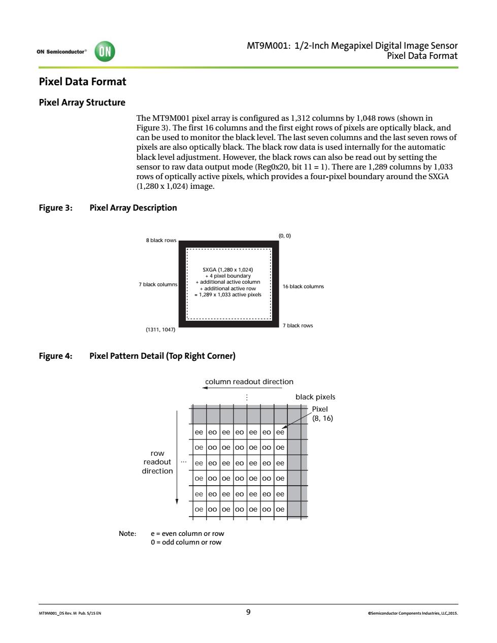
ON MT9M001:1/2-Inch Megapixel Digital Im Pixel Data Format Pixel Array Structure and the f pixels are also optically black.The black row data is used internally for the automatic black level adjustment.However,the black rows can also be read out by setting the sensor to raw .280x 1024)image oundary around Figure 3: Pixel Array Description 8 black rov 6 bla 31,1047 olack row Figure 4: Pixel Pattern Detail(Top Right Corner) column readout direction black pixels Pixel (8,16) ee eoee eo ee eoee oe oo oe oooeoooe row lee eoeeeo ee eo oe oo oe oo oe oo eo ee eo ee eo oe oooe Note: 8=8a.cltmorow
MT9M001_DS Rev. M Pub. 5/15 EN 9 ©Semiconductor Components Industries, LLC,2015. MT9M001: 1/2-Inch Megapixel Digital Image Sensor Pixel Data Format Pixel Data Format Pixel Array Structure The MT9M001 pixel array is configured as 1,312 columns by 1,048 rows (shown in Figure 3). The first 16 columns and the first eight rows of pixels are optically black, and can be used to monitor the black level. The last seven columns and the last seven rows of pixels are also optically black. The black row data is used internally for the automatic black level adjustment. However, the black rows can also be read out by setting the sensor to raw data output mode (Reg0x20, bit 11 = 1). There are 1,289 columns by 1,033 rows of optically active pixels, which provides a four-pixel boundary around the SXGA (1,280 x 1,024) image. Figure 3: Pixel Array Description Figure 4: Pixel Pattern Detail (Top Right Corner) Note: e = even column or row 0 = odd column or row (1311, 1047) 16 black columns 7 black rows 8 black rows (0, 0) 7 black columns SXGA (1,280 x 1,024) + 4 pixel boundary + additional active column + additional active row = 1,289 x 1,033 active pixels Pixel (8, 16) black pixels column readout direction . . . . row readout direction ee oe ee oe ee oe eo oo eo oo eo oo ee oe ee oe ee oe eo oo eo oo eo oo ee oe ee oe ee oe eo oo eo oo eo oo ee oe ee oe ee oe
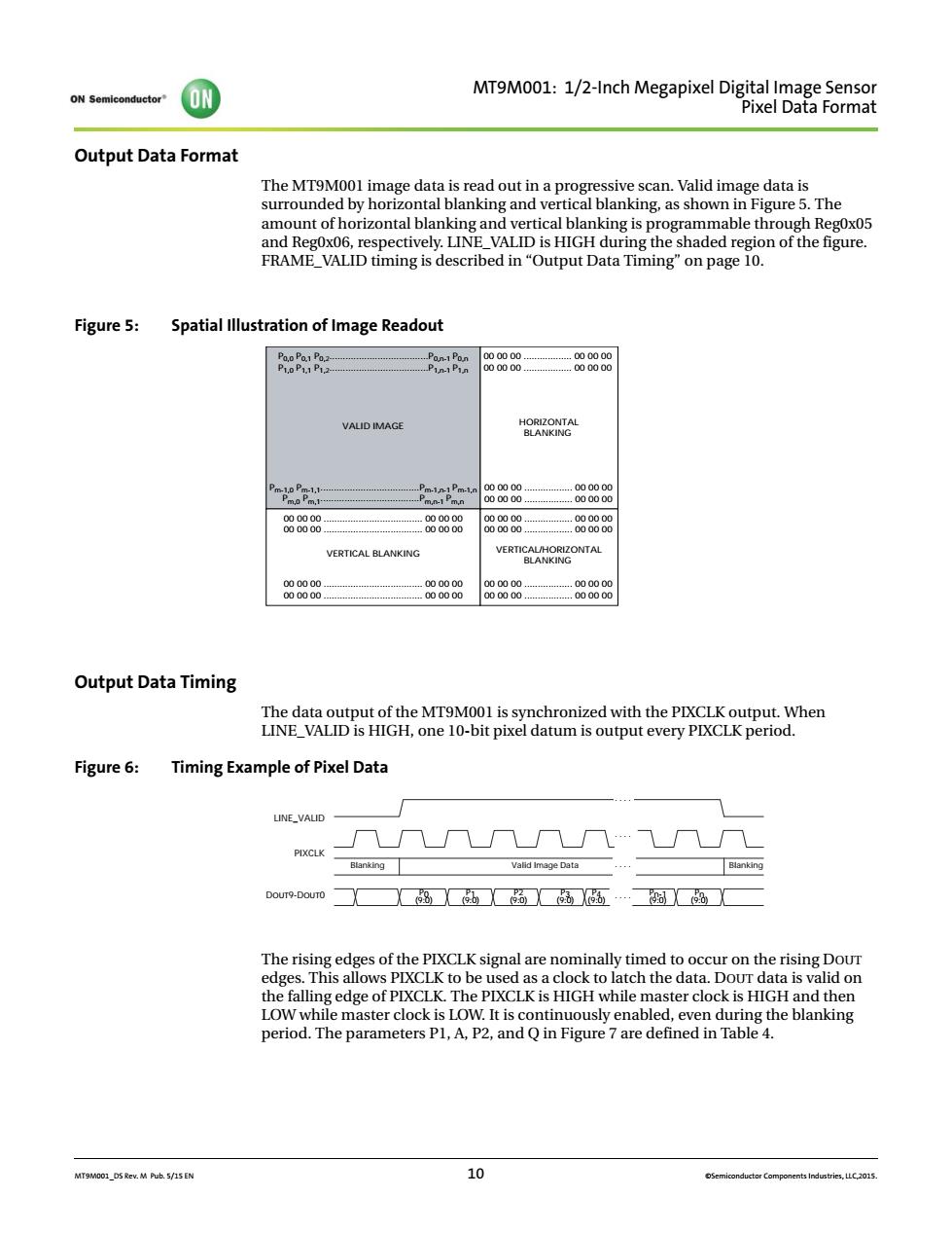
MT9M001:1/2-Inch Megapixel Digital Ima Output Data Format amount of horizontal blanking and vertical blanking is p rogrammable through Reg0x05 and RegOx06,respectively.LINE_VALID is HIGH during the shaded region of the figure. FRAME_VALID timing is described in"Output Data Timing"on page 10. Figure 5:Spatial lllustration of Image Readout VALID MAGE LANDIA 88888 VERTICAL BLANKING 60a88=898868 Output Data Timing UNVADece Figure 6:Timing Example of Pixel Data UNE_VALD- 几U几U八U八ni inallu timed the falling edge of PIXCLK.The PIXCLK is HIGH while master clock is HIGH and then M hS EN 6
MT9M001_DS Rev. M Pub. 5/15 EN 10 ©Semiconductor Components Industries, LLC,2015. MT9M001: 1/2-Inch Megapixel Digital Image Sensor Pixel Data Format Output Data Format The MT9M001 image data is read out in a progressive scan. Valid image data is surrounded by horizontal blanking and vertical blanking, as shown in Figure 5. The amount of horizontal blanking and vertical blanking is programmable through Reg0x05 and Reg0x06, respectively. LINE_VALID is HIGH during the shaded region of the figure. FRAME_VALID timing is described in “Output Data Timing” on page 10. Figure 5: Spatial Illustration of Image Readout Output Data Timing The data output of the MT9M001 is synchronized with the PIXCLK output. When LINE_VALID is HIGH, one 10-bit pixel datum is output every PIXCLK period. Figure 6: Timing Example of Pixel Data The rising edges of the PIXCLK signal are nominally timed to occur on the rising DOUT edges. This allows PIXCLK to be used as a clock to latch the data. DOUT data is valid on the falling edge of PIXCLK. The PIXCLK is HIGH while master clock is HIGH and then LOW while master clock is LOW. It is continuously enabled, even during the blanking period. The parameters P1, A, P2, and Q in Figure 7 are defined in Table 4. P0,0 P0,1 P0,2.P0,n-1 P0,n P1,0 P1,1 P1,2.P1,n-1 P1,n 00 00 00 . 00 00 00 00 00 00 . 00 00 00 Pm-1,0 Pm-1,1.Pm-1,n-1 Pm-1,n Pm,0 Pm,1.Pm,n-1 Pm,n 00 00 00 . 00 00 00 00 00 00 . 00 00 00 00 00 00 . 00 00 00 00 00 00 . 00 00 00 00 00 00 . 00 00 00 00 00 00 . 00 00 00 00 00 00 . 00 00 00 00 00 00 . 00 00 00 00 00 00 . 00 00 00 00 00 00 . 00 00 00 VALID IMAGE HORIZONTAL BLANKING VERTICAL BLANKING VERTICAL/HORIZONTAL BLANKING LINE_VALID PIXCLK DOUT9-DOUT0 . . . . . . . . . . . . . . . . P0 (9:0) P1 (9:0) P2 (9:0) P3 (9:0) P4 (9:0) Pn-1 (9:0) Pn (9:0) Blanking Valid Image Data Blanking