
Laboratory Exercise 1 Switches,Lights,and Multiplexers 恤 uses these ve wi PartI The DE2 boa L uses these switches and shows their states on the LEDs.Since there are switches and lights it is convenien 2RapRRkseie大semmcnari LEDR(17)<=SW(17): LEDR(16)<=SW(16): LEDR(0)<=SW(0): n LEDR DE2 User Manal.For example,the manual specifies that SWo is connected to the FPGA pin N25 and LEDRo is ke the pin as d HDL esign which isas fromAltera It isimportant to realire that the pin assignments in pin names given ed in The file uses th es in Figure I (note that the Quartus II software nts,while the VHDL syntax uses()round brackets). 6eyt恤coe6你8Whh眼es In STD LOGIC VECTORU7 DOWNTO ON LEDR:OUT STDLOGIC_VECTOR(17 DOWNTO0)):--red LEDs END partl; LEDR <-SW; END Behavior
Laboratory Exercise 1 Switches, Lights, and Multiplexers The purpose of this exercise is to learn how to connect simple input and output devices to an FPGA chip and implement a circuit that uses these devices. We will use the switches SW17−0 on the DE2 board as inputs to the circuit. We will use light emitting diodes (LEDs) and 7-segment displays as output devices. Part I The DE2 board provides 18 toggle switches, called SW17−0, that can be used as inputs to a circuit, and 18 red lights, called LEDR17−0, that can be used to display output values. Figure 1 shows a simple VHDL entity that uses these switches and shows their states on the LEDs. Since there are 18 switches and lights it is convenient to represent them as arrays in the VHDL code, as shown. We have used a single assignment statement for all 18 LEDR outputs, which is equivalent to the individual assignments LEDR(17) <= SW(17); LEDR(16) <= SW(16); ... LEDR(0) <= SW(0); The DE2 board has hardwired connections between its FPGA chip and the switches and lights. To use SW 17−0 and LEDR17−0 it is necessary to include in your Quartus II project the correct pin assignments, which are given in the DE2 User Manual. For example, the manual specifies that SW0 is connected to the FPGA pin N25 and LEDR0 is connected to pin AE23. A good way to make the required pin assignments is to import into the Quartus II software the file called DE2 pin assignments.csv, which is provided on the DE2 System CD and in the University Program section of Altera’s web site. The procedure for making pin assignments is described in the tutorial Quartus II Introduction using VHDL Design, which is also available from Altera. It is important to realize that the pin assignments in the DE2 pin assignments.csv file are useful only if the pin names given in the file are exactly the same as the port names used in your VHDL entity. The file uses the names SW[0] ... SW[17] and LEDR[0] ... LEDR[17] for the switches and lights, which is the reason we used these names in Figure 1 (note that the Quartus II software uses [ ] square brackets for array elements, while the VHDL syntax uses ( ) round brackets). LIBRARY ieee; USE ieee.std logic 1164.all; - - Simple module that connects the SW switches to the LEDR lights ENTITY part1 IS PORT ( SW : IN STD LOGIC VECTOR(17 DOWNTO 0); LEDR : OUT STD LOGIC VECTOR(17 DOWNTO 0)); - - red LEDs END part1; ARCHITECTURE Behavior OF part1 IS BEGIN LEDR <= SW; END Behavior 1
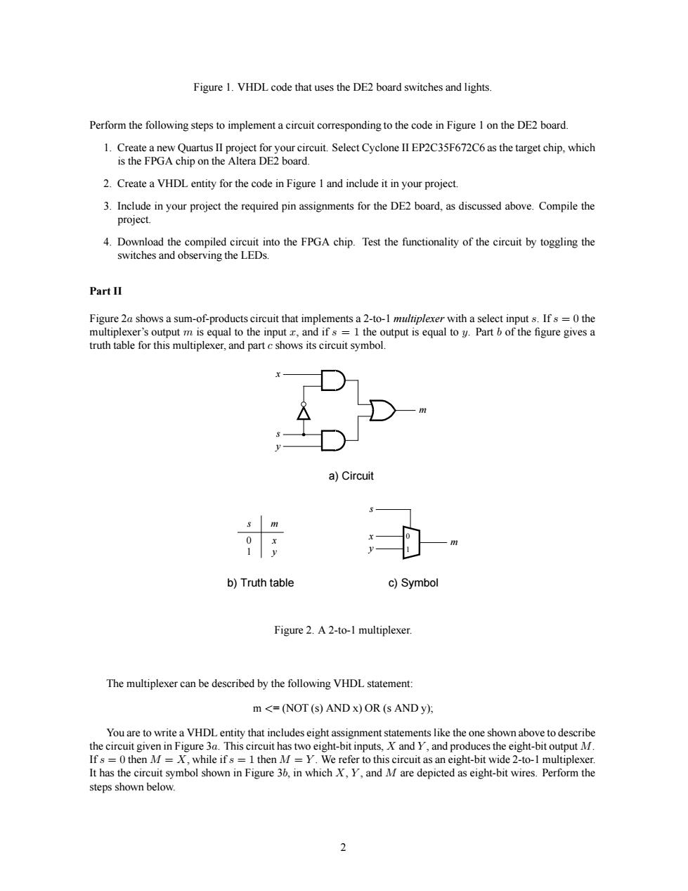
Figure 1.VHDLcode that uses the DE2 board switches and lights Perform the following steps to implement a circuit corresponding to the code in Figure 1on the DE2 board. 2.Create a VHDL entity for the code in Figure I and include it inyour project 3.Include in your project the required pin assignments for the DE2 board,as discussed above.Compile the project. 4.Download the compiled circuit into the FPGA chip.Test the functionality of the circuit by toggling the switches and observing the LEDs. Figure 2a shows a sum-of-products circuit that implements a 2-to-1 multiplexer with a select input s.If s =0 the multiplexer's outputm is equal to the input and ifs1 the output is equal toy Partof the figure gives a truth table for this multiplexer,and partcshows its circuit symbol. 一m a)Circuit s m b)Truth table c)Symbol Figure 2.A 2-to-1 multiplexer The multiplexer can be described by the following VHDL statement. m <=(NOT (s)AND x)OR(s ANDy): You are to writea VHDL entity that includes eight assignment statements like the one shown above to describe This circuit has two eight-bit inputs.X and Y.and pro ces th eight-bit output A It has the uit symbol sho e3地n which.,ane an eight-bi t-bit res.Perform the steps shown below. 2
Figure 1. VHDL code that uses the DE2 board switches and lights. Perform the following steps to implement a circuit corresponding to the code in Figure 1 on the DE2 board. 1. Create a new Quartus II project for your circuit. Select Cyclone II EP2C35F672C6 as the target chip, which is the FPGA chip on the Altera DE2 board. 2. Create a VHDL entity for the code in Figure 1 and include it in your project. 3. Include in your project the required pin assignments for the DE2 board, as discussed above. Compile the project. 4. Download the compiled circuit into the FPGA chip. Test the functionality of the circuit by toggling the switches and observing the LEDs. Part II Figure 2a shows a sum-of-products circuit that implements a 2-to-1 multiplexer with a select input s. If s = 0 the multiplexer’s output m is equal to the input x, and if s = 1 the output is equal to y. Part b of the figure gives a truth table for this multiplexer, and part c shows its circuit symbol. x s y 0 1 x s y m m s m 0 1 x y a) Circuit b) Truth table c) Symbol Figure 2. A 2-to-1 multiplexer. The multiplexer can be described by the following VHDL statement: m <= (NOT (s) AND x) OR (s AND y); You are to write a VHDL entity that includes eight assignment statements like the one shown above to describe the circuit given in Figure 3a. This circuit has two eight-bit inputs, X and Y , and produces the eight-bit output M. If s = 0 then M = X, while if s = 1 then M = Y . We refer to this circuit as an eight-bit wide 2-to-1 multiplexer. It has the circuit symbol shown in Figure 3b, in which X, Y , and M are depicted as eight-bit wires. Perform the steps shown below. 2
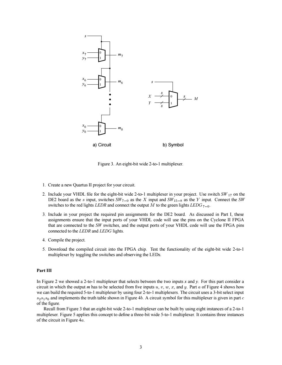
a)Circuit b)Symbol Figure 3.An eight-bit wide 2-to-1 multiplexer. 1.Create a new Quartus l project for your circuit swithes to the red lightsRand conect the outputMto the green lightsG 3.Include in your project the required pin assignments for the DE2 board.As discussed in Part I,these 4.Compile the project 5.Download the compiled circuit into the FPGA chip.Test the functionality of the eight-bit wide 2-to-1 multiplexer by togging the switches and observing the LEDs. PartII 盛omp eight-bit vide 2-to-1 insta oteecmng5ees multiplexe ia
0 1 s a) Circuit b) Symbol 0 1 0 1 m0 m6 m7 x6 x0 y6 y0 y7 x7 0 1 s M Y X 8 8 8 Figure 3. An eight-bit wide 2-to-1 multiplexer. 1. Create a new Quartus II project for your circuit. 2. Include your VHDL file for the eight-bit wide 2-to-1 multiplexer in your project. Use switch SW 17 on the DE2 board as the s input, switches SW7−0 as the X input and SW15−8 as the Y input. Connect the SW switches to the red lights LEDR and connect the output M to the green lights LEDG7−0. 3. Include in your project the required pin assignments for the DE2 board. As discussed in Part I, these assignments ensure that the input ports of your VHDL code will use the pins on the Cyclone II FPGA that are connected to the SW switches, and the output ports of your VHDL code will use the FPGA pins connected to the LEDR and LEDG lights. 4. Compile the project. 5. Download the compiled circuit into the FPGA chip. Test the functionality of the eight-bit wide 2-to-1 multiplexer by toggling the switches and observing the LEDs. Part III In Figure 2 we showed a 2-to-1 multiplexer that selects between the two inputs x and y. For this part consider a circuit in which the output m has to be selected from five inputs u, v, w, x, and y. Part a of Figure 4 shows how we can build the required 5-to-1 multiplexer by using four 2-to-1 multiplexers. The circuit uses a 3-bit select input s2s1s0 and implements the truth table shown in Figure 4b. A circuit symbol for this multiplexer is given in part c of the figure. Recall from Figure 3 that an eight-bit wide 2-to-1 multiplexer can be built by using eight instances of a 2-to-1 multiplexer. Figure 5 applies this concept to define a three-bit wide 5-to-1 multiplexer. It contains three instances of the circuit in Figure 4a. 3
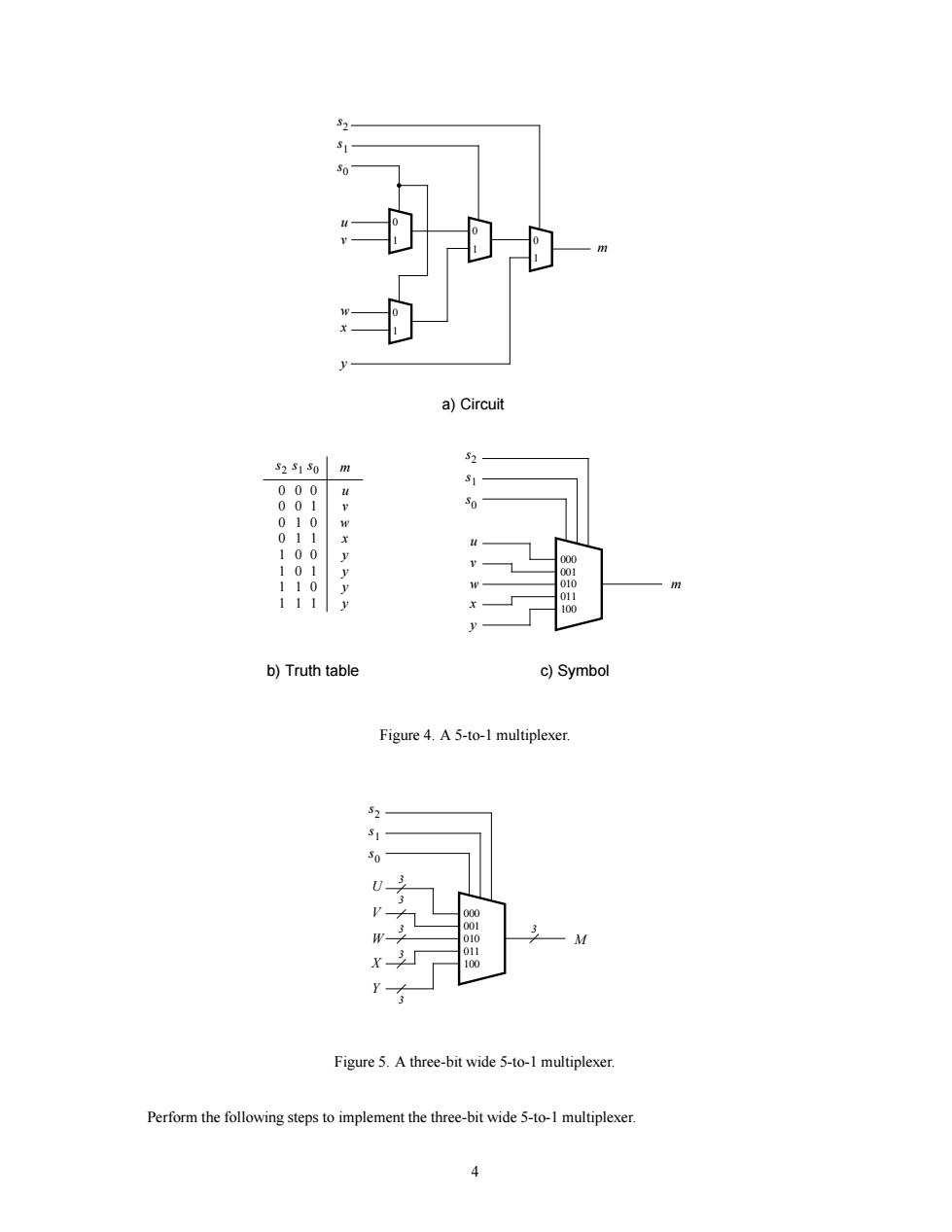
a)Circuit 32s150m 拍出 b)Truth table c)Symbol Figure 4.A 5-to-1 multiplexer Figure 5.A three-bit wide 5-to-1 multiplexer Perform the following steps to implement the three-bit wide 5-to-1 multiplexer
0 1 a) Circuit 0 1 0 1 w x v u 000 m 0 1 s1 s2 s0 y m 001 010 011 100 s1 s2 s0 w x v u y c) Symbol m 0 0 u v b) Truth table s1 s0 s2 0 0 0 1 0 0 w x 1 0 1 1 1 0 0 y 1 1 0 1 1 0 111 y y y Figure 4. A 5-to-1 multiplexer. 000 M 001 010 011 100 s1 s2 s0 W X V U Y 3 3 3 3 3 3 Figure 5. A three-bit wide 5-to-1 multiplexer. Perform the following steps to implement the three-bit wide 5-to-1 multiplexer. 4
1.Create a new Quartus ll project for your circuit. the Sswitches to the red lights LEDR and connect the output M to the green lightsLEDG 3.Include in your project the required pin assignments for the DE2 board.Compile the project. 4.Download the compiled circuit into the FPGA chip.Test the functionality of the three-bit wide 5-to- es and observing the LEDs.Ensure that each of the inputs U to Y can be outpu PartIV .This decoder producess To kena the d (plus theblank'character,which is selected for codes100-111). esegments in the display are identifed by the ind to o shown in the figure.Each segment s riving it to the logie va moLrcodciospecifCaehi1ogicfincionLsigaBolcanec nression Figure6.A7-segment decoder cacico Character 000 001 Table 1.Character codes. Perform the following steps: 1.Create a new Quartus lI project for your circuit
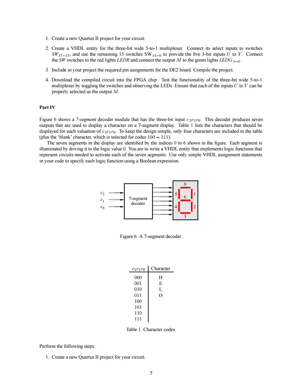
1. Create a new Quartus II project for your circuit. 2. Create a VHDL entity for the three-bit wide 5-to-1 multiplexer. Connect its select inputs to switches SW17−15, and use the remaining 15 switches SW14−0 to provide the five 3-bit inputs U to Y . Connect the SW switches to the red lights LEDR and connect the output M to the green lights LEDG 2−0. 3. Include in your project the required pin assignments for the DE2 board. Compile the project. 4. Download the compiled circuit into the FPGA chip. Test the functionality of the three-bit wide 5-to-1 multiplexer by toggling the switches and observing the LEDs. Ensure that each of the inputs U to Y can be properly selected as the output M. Part IV Figure 6 shows a 7-segment decoder module that has the three-bit input c 2c1c0. This decoder produces seven outputs that are used to display a character on a 7-segment display. Table 1 lists the characters that should be displayed for each valuation of c2c1c0. To keep the design simple, only four characters are included in the table (plus the ‘blank’ character, which is selected for codes 100 − 111). The seven segments in the display are identified by the indices 0 to 6 shown in the figure. Each segment is illuminated by driving it to the logic value 0. You are to write a VHDL entity that implements logic functions that represent circuits needed to activate each of the seven segments. Use only simple VHDL assignment statements in your code to specify each logic function using a Boolean expression. 7-segment 0 1 2 3 4 5 6 decoder c2 c1 c0 Figure 6. A 7-segment decoder. c2c1c0 Character 000 H 001 E 010 L 011 O 100 101 110 111 Table 1. Character codes. Perform the following steps: 1. Create a new Quartus II project for your circuit. 5