
TOSHIBA The Change of IGBT Package for Strobe Flasher (Unit in mm) TO-220 Class DP SOP-8 TSSOP-8 10.3 MAX Changed to Compact Package 6.4 BBRB 4.4 0109 T T0-220SM 5.5MAX 10.3 MAX 20+51 不 L6.8 MAX 2.5 MAX T0-220FL 2003 Dec DP054001101 6/22
6/22 2003 Dec DP0540011_01 Thru-Hole Type SMD Type (Unit in : mm) DP The Change of IGBT Package for Strobe Flasher TO-220 Class SOP-8 TSSOP-8 Changed to Compact Package TO-220FL TO-220SM 2.5 10.3 MAX 10.6 MAX 10.3 MAX 10.6 MAX 6.8 MAX 5.5 2.5 MAX 4.4 ±0.2 6.0 ±0.3 5.5MAX. 1.5 ±0.2 3.0 6.4 4.4 0.85 ±0.05
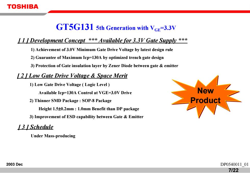
TOSHIBA GT5G131 5th Generation with VGE=3.3V [1 Development Concept **Available for 3.3V Gate Supply ** 1)Achievement of 3.0V Minimum Gate Drive Voltage by latest design rule 2)Guarantee of Maximum Icp=130A by optimized trench gate design 3)Protection of Gate insulation layer by Zener Diode between gate emitter I2 I Low Gate Drive Voltage Space Merit 1)Low Gate Drive Voltage Logic Level) Available Icp=130A Control at VGE=3.0V Drive 2)Thinner SMD Package:SOP-8 Package Height 1.540.2mm 1.0mm Benefit than DP package 3)Improvement of ESD capability between Gate Emitter 13 ISchedule Under Mass-producing 2003 Dec DP054001101 7122
7/22 2003 Dec DP0540011_01 [ 1 ] Development Concept *** Available for 3.3V Gate Supply *** 1) Achievement of 3.0V Minimum Gate Drive Voltage by latest design rule 2) Guarantee of Maximum Icp=130A by optimized trench gate design 3) Protection of Gate insulation layer by Zener Diode between gate & emitter [ 2 ] Low Gate Drive Voltage & Space Merit 1) Low Gate Drive Voltage ( Logic Level ) Available Icp=130A Control at VGE=3.0V Drive 2) Thinner SMD Package : SOP-8 Package Height 1.5±0.2mm : 1.0mm Benefit than DP package 3) Improvement of ESD capability between Gate & Emitter [ 3 ] Schedule Under Mass-producing GT5G131 5th Generation with VGE=3.3V New Product New Product
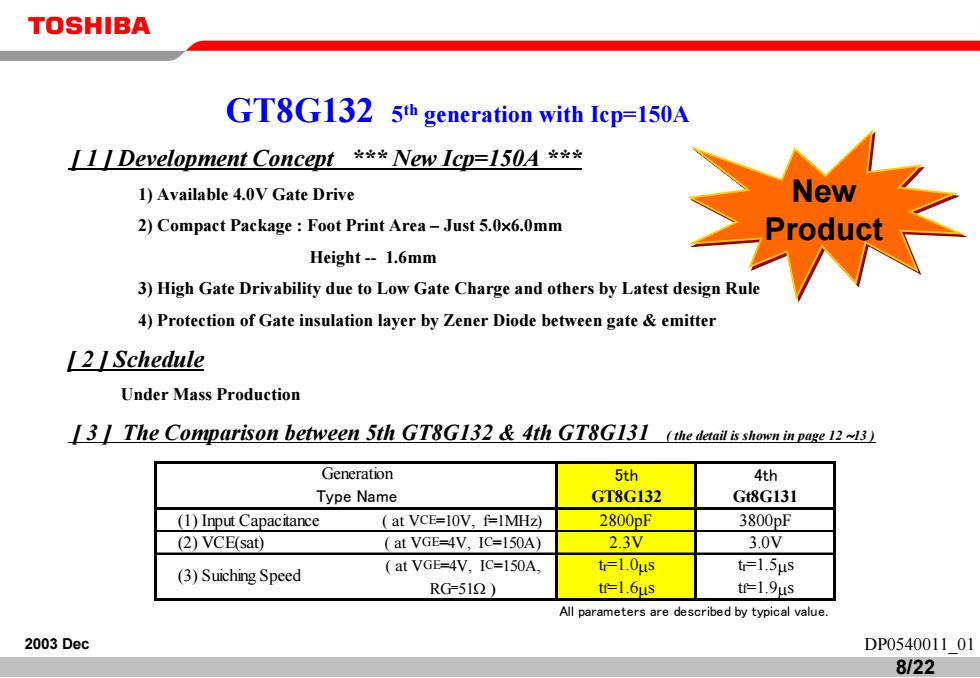
TOSHIBA GT8G132 5th generation with Icp=150A [1|Development Concept **New Icp=150A ** 1)Available 4.0V Gate Drive 2)Compact Package:Foot Print Area-Just 5.0x6.0mm Height-1.6mm 3)High Gate Drivability due to Low Gate Charge and others by Latest design Rule 4)Protection of Gate insulation layer by Zener Diode between gate emitter 12 ISchedule Under Mass Production 13The Comparison between 5th GT8G132 4th GT8G131 (the daail is showun inpage 12~13) Generation 5th 4th Type Name GT8G132 Gt8G131 (1)Input Capacitance at VCE=10V.f=1MHz) 2800pF 3800pF (2)VCE(sat) at VGE=4V,IC=150A) 2.3V 3.0V (3)Suiching Speed at VGE=4V,IC=150A, tr=1.OuS t=1.5us RG=51) tf=1.6us te19μs All parameters are described by typical value. 2003 Dec DP054001101 8/22
8/22 2003 Dec DP0540011_01 [ 1 ] Development Concept *** New Icp=150A *** 1) Available 4.0V Gate Drive 2) Compact Package : Foot Print Area – Just 5.0×6.0mm Height - 1.6mm 3) High Gate Drivability due to Low Gate Charge and others by Latest design Rule 4) Protection of Gate insulation layer by Zener Diode between gate & emitter [ 2 ] Schedule Under Mass Production [ 3 ] The Comparison between 5th GT8G132 & 4th GT8G131 ( the detail is shown in page 12 ∼13 ) GT8G132 5th generation with Icp=150A New Product New Product 5th 4th GT8G132 Gt8G131 (1) Input Capacitance ( at VCE=10V, f=1MHz) 2800pF 3800pF (2) VCE(sat) ( at VGE=4V, IC=150A) 2.3V 3.0V ( at VGE=4V, IC=150A, tr=1.0µs tr=1.5µs RG=51Ω ) tf=1.6µs tf=1.9µs Generation Type Name All parameters are described by typical value. (3) Suiching Speed