
ISHAY IRFP450,SiHFP450 Vishay Siliconix Power MOSFET PRODUCT SUMMARY FEATURES Rating s(V) 500 ⑧ (on)( Vas 10V 0.40 che Ratec (nc ntral Mounting Hole RoHS Fast Sv Ease of Par ing Simple Drive Requirements Lead (Pb)-free Available T0-247 DESCRIPTION ruggedized device design.low on-resistance and commerial-industria 8-220dey es.The TO-247 is similar but superior to the N-Channel MOSFET greater creepage d between pins to meet the requirements of most safety specifications. ORDERING INFORMATION Package Lead(Pb)-free SiHFP450-E3 SnPb SIHFP450 ABSOLUTE MAXIMUM RATINGS Tc =25C,unless otherwise noted PARAMETER SYMBOL LIMIT UNIT Drain-Source Voltage Vos 500 Gate-Source Voltage VGs ±20 Continuous Drain Current lo 87 Linear Derating Factor 15 W/PC EAS 760 m Tc=25℃ 190 Peak Diode Recovery dV/dts dV/dt 3.5 Vins Operating Junction and Storage Temperature Range TJ,Tsta -55to+150 Soldering Recommendations (Peak Temperature) for 10s 0 Mounting Torque 6-32 or M3 screw Notes d.1.6 mm from case. Pb containing terminations are not RoHS compliant,exemptions may apply 127160 www.vishay.com
Document Number: 91233 www.vishay.com S-81271-Rev. A, 16-Jun-08 1 Power MOSFET IRFP450, SiHFP450 Vishay Siliconix FEATURES • Dynamic dV/dt Rating • Repetitive Avalanche Rated • Isolated Central Mounting Hole • Fast Switching • Ease of Paralleling • Simple Drive Requirements • Lead (Pb)-free Available DESCRIPTION Third generation Power MOSFETs from Vishay provide the designer with the best combination of fast switching, ruggedized device design, low on-resistance and cost-effectiveness. The TO-247 package is preferred for commercial-industrial applications where higher power levels preclude the use of TO-220 devices. The TO-247 is similar but superior to the earlier TO-218 package because its isolated mounting hole. It also provides greater creepage distances between pins to meet the requirements of most safety specifications. Notes a. Repetitive rating; pulse width limited by maximum junction temperature (see fig. 11). b. VDD = 50 V, starting TJ = 25 °C, L = 7.0 mH, RG = 25 Ω, IAS = 14 A (see fig. 12). c. ISD ≤ 14 A, dI/dt ≤ 130 A/µs, VDD ≤ VDS, TJ ≤ 150 °C. d. 1.6 mm from case. PRODUCT SUMMARY VDS (V) 500 RDS(on) (Ω) VGS = 10 V 0.40 Qg (Max.) (nC) 150 Qgs (nC) 20 Qgd (nC) 80 Configuration Single N-Channel MOSFET G D S TO-247 G D S Available RoHS* COMPLIANT ORDERING INFORMATION Package TO-247 Lead (Pb)-free IRFP450PbF SiHFP450-E3 SnPb IRFP450 SiHFP450 ABSOLUTE MAXIMUM RATINGS TC = 25 °C, unless otherwise noted PARAMETER SYMBOL LIMIT UNIT Drain-Source Voltage VDS 500 V Gate-Source Voltage VGS ± 20 Continuous Drain Current VGS at 10 V TC = 25 °C ID 14 TC = 100 °C 8.7 A Pulsed Drain Currenta IDM 56 Linear Derating Factor 1.5 W/°C Single Pulse Avalanche Energyb EAS 760 mJ Repetitive Avalanche Currenta IAR 8.7 A Repetitive Avalanche Energya EAR 19 mJ Maximum Power Dissipation TC = 25 °C PD 190 W Peak Diode Recovery dV/dtc dV/dt 3.5 V/ns Operating Junction and Storage Temperature Range TJ, Tstg - 55 to + 150 °C Soldering Recommendations (Peak Temperature) for 10 s 300d Mounting Torque 6-32 or M3 screw 10 lbf · in 1.1 N · m * Pb containing terminations are not RoHS compliant, exemptions may apply
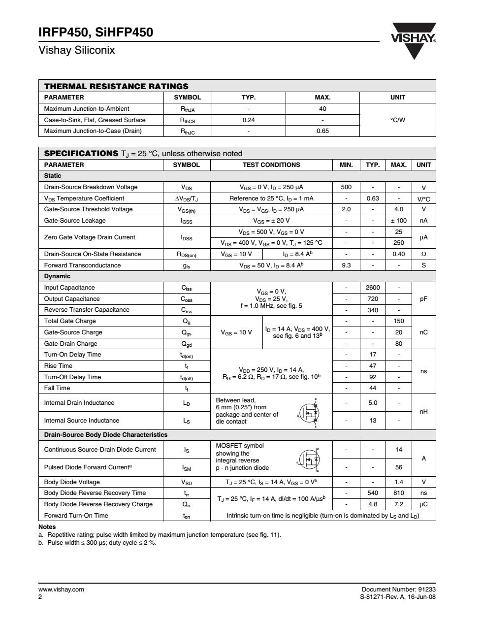
IRFP450,SiHFP450 VISHAY Vishay Siliconix THERMAL RESISTANCE RATINGS AMETER TYP. MAX UNIT on-to- 40 se-to-Sink,Flat,Grea ed Surface 0.24 Maximum Junction-to-Case (Drain) 0.65 SPECIFICATIONS TJ=25C,unless otherwise noted PARAMETER SYMBOL TEST CONDITIONS MIN.TYP.MAX.UNIT Static Drain-Source Breakdown Voltage Vos VGs =0 V,lo =250 MA 500··v Vos/Tj 025℃,lb=1m 0.63 rce Thresh Vas(h) Vos=Vas.Ip=250 HA 2.0 4.0 Gate-Source Leakage IGss VGs■±20V ±100nA Vps =500 V.VGs =0V 25 Zero Gate Voltage Drain Current loss Vos 400 V,Vos =0V.T 125C 250 A Drain-Source On-State Resistance VGs =10V In=8.4AD 0.400 Forward Transconductance Vos=50V,lb=8.4A地 93 Dynamic Input Capacitance 2600 Output Capacitance Capacitance 340 150 Gate-Source Charge Vas-10V 41 20 nC Gate-Drain Charge 0g 80 Turn-On Delay Time 17 Rise Time 47 ns Turn-Oft Delay Time Ro1 Fall Time 44 Intemal Drain Inductance 名 5.0 nH 13 Drain-Source Body Diode Characteristics Continuous Source-Drain Diode Current 14 Pulsed Diode Forward Currente 56 Body Diode Voltage T1=25℃.s=14AVG5=00 1.4y Body Diode Reverse Recovery Time 540810ns T=25C.Ie=14 A.dl/dt 100 A/usb Body Diode Reverse Recovery Charge 4.87.2uC vard Tumn-On Time Intrinsic tum-on time is negligible (tum-on is do nated by Ls and Lo) Repet www.vishay.com g8R688
www.vishay.com Document Number: 91233 2 S-81271-Rev. A, 16-Jun-08 IRFP450, SiHFP450 Vishay Siliconix Notes a. Repetitive rating; pulse width limited by maximum junction temperature (see fig. 11). b. Pulse width ≤ 300 µs; duty cycle ≤ 2 %. THERMAL RESISTANCE RATINGS PARAMETER SYMBOL TYP. MAX. UNIT Maximum Junction-to-Ambient RthJA - 40 Case-to-Sink, Flat, Greased Surface RthCS 0.24 - °C/W Maximum Junction-to-Case (Drain) RthJC - 0.65 SPECIFICATIONS TJ = 25 °C, unless otherwise noted PARAMETER SYMBOL TEST CONDITIONS MIN. TYP. MAX. UNIT Static Drain-Source Breakdown Voltage VDS VGS = 0 V, ID = 250 µA 500 - - V VDS Temperature Coefficient ΔVDS/TJ Reference to 25 °C, ID = 1 mA - 0.63 - V/°C Gate-Source Threshold Voltage VGS(th) VDS = VGS, ID = 250 µA 2.0 - 4.0 V Gate-Source Leakage IGSS VGS = ± 20 V - - ± 100 nA Zero Gate Voltage Drain Current IDSS VDS = 500 V, VGS = 0 V - - 25 µA VDS = 400 V, VGS = 0 V, TJ = 125 °C - - 250 Drain-Source On-State Resistance RDS(on) VGS = 10 V ID = 8.4 Ab - - 0.40 Ω Forward Transconductance gfs VDS = 50 V, ID = 8.4 Ab 9.3 - - S Dynamic Input Capacitance Ciss VGS = 0 V, VDS = 25 V, f = 1.0 MHz, see fig. 5 - 2600 - Output Capacitance Coss - 720 - pF Reverse Transfer Capacitance Crss - 340 - Total Gate Charge Qg VGS = 10 V ID = 14 A, VDS = 400 V, see fig. 6 and 13b - - 150 Gate-Source Charge Qgs - - 20 nC Gate-Drain Charge Qgd - - 80 Turn-On Delay Time td(on) VDD = 250 V, ID = 14 A, RG = 6.2 Ω, RD = 17 Ω, see fig. 10b - 17 - ns Rise Time tr - 47 - Turn-Off Delay Time td(off) - 92 - Fall Time tf - 44 - Internal Drain Inductance LD Between lead, 6 mm (0.25") from package and center of die contact - 5.0 - nH Internal Source Inductance LS - 13 - Drain-Source Body Diode Characteristics Continuous Source-Drain Diode Current IS MOSFET symbol showing the integral reverse p - n junction diode - - 14 A Pulsed Diode Forward Currenta ISM - - 56 Body Diode Voltage VSD TJ = 25 °C, IS = 14 A, VGS = 0 Vb - - 1.4 V Body Diode Reverse Recovery Time trr TJ = 25 °C, IF = 14 A, dI/dt = 100 A/µsb - 540 810 ns Body Diode Reverse Recovery Charge Qrr - 4.8 7.2 µC Forward Turn-On Time ton Intrinsic turn-on time is negligible (turn-on is dominated by LS and LD) D S G S D G

VISHAY IRFP450,SiHFP450 Vishay Siliconix TYPICAL CHARACTERISTICS 25C,unless otherwise noted Vos.Drain-to-Source Voltage(volts) Ves.Gate-to-Source Voltage (volts) Fig.1-Typical Output Characteristics,Te =25C Fig.3-Typical Transfer Characteristics VG 0 Vos,Drain-to-Source Voltage (volts) aure(c Fig.2-Typical Output Characteristics,Tc=150c Fig.4-Nor 8o29969128 ww.vishay.com
Document Number: 91233 www.vishay.com S-81271-Rev. A, 16-Jun-08 3 IRFP450, SiHFP450 Vishay Siliconix TYPICAL CHARACTERISTICS 25 °C, unless otherwise noted Fig. 1 - Typical Output Characteristics, TC = 25 °C Fig. 2 - Typical Output Characteristics, TC = 150 °C Fig. 3 - Typical Transfer Characteristics Fig. 4 - Normalized On-Resistance vs. Temperature

IRFP450,SiHFP450 VISHAY Vishay Siliconix Cod.Cas SHORTE √so.Source-to-Drain Voltage(vols】 Fig.5-Typl ig.7-Typ ical Source-Drain Diode Forward volta G.Total Gate Charge (nC) Ds.Dr volts Fig.6-Typical Gate Charge vs.Gate-to urce Voltage mum Sa ting Are www.vishay.com S9827R风69a
www.vishay.com Document Number: 91233 4 S-81271-Rev. A, 16-Jun-08 IRFP450, SiHFP450 Vishay Siliconix Fig. 5 - Typical Capacitance vs. Drain-to-Source Voltage Fig. 6 - Typical Gate Charge vs. Gate-to-Source Voltage Fig. 7 - Typical Source-Drain Diode Forward Voltage Fig. 8 - Maximum Safe Operating Area
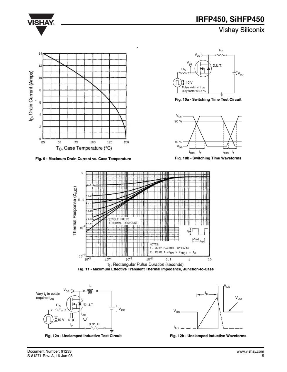
VISHAY IRFP450,SiHFP450 Vishay Siliconix (左1ov Fig.10a-Switching Time e Test Circui Tc.Case Temperature(C) Fig.9-Maximum Drain Current vs.Case Temperature Fig.10b-Switching Time Waveforms OUTY FACTOR,D-ti/t PEAK T:-PON x ZthjcTc Fig.11-Maximum ec Junction-to-Case Vos As- Fig.12a-Unclamped Inductive Test Circuit Fig.12b-Unclamped Inductive Waveforms 8o29969128
Document Number: 91233 www.vishay.com S-81271-Rev. A, 16-Jun-08 5 IRFP450, SiHFP450 Vishay Siliconix Fig. 9 - Maximum Drain Current vs. Case Temperature Fig. 10a - Switching Time Test Circuit Fig. 10b - Switching Time Waveforms Fig. 11 - Maximum Effective Transient Thermal Impedance, Junction-to-Case Fig. 12a - Unclamped Inductive Test Circuit Fig. 12b - Unclamped Inductive Waveforms Pulse width ≤ 1 µs Duty factor ≤ 0.1 % RD VGS RG D.U.T. 10 V + - VDS VDD VDS 90 % 10 % VGS t d(on) t r t d(off) t f RG IAS tp 0.01 Ω D.U.T L VDS + - VDD A 10 V Vary tp to obtain required IAS IAS VDS VDD VDS tp