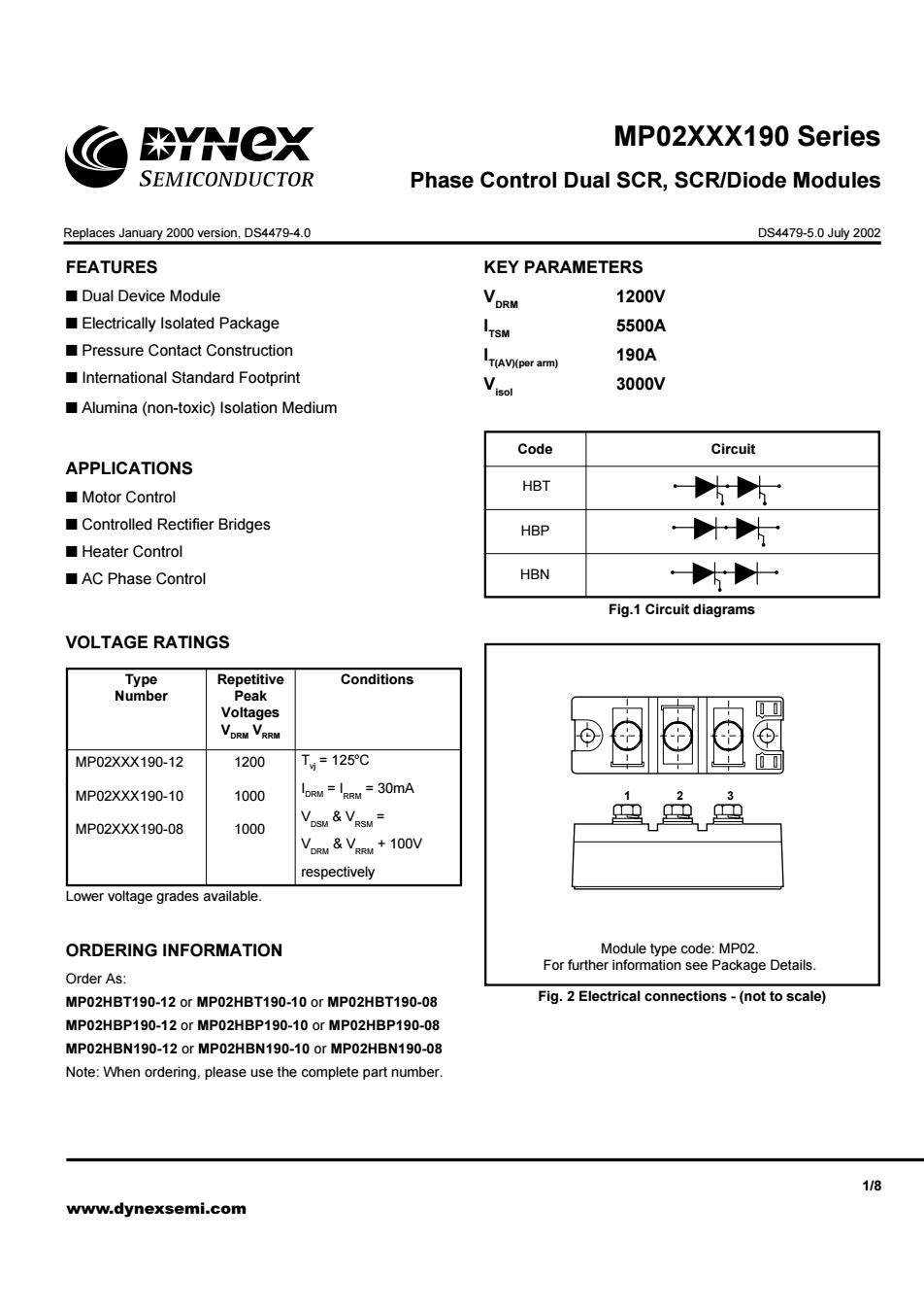
BYNex MP02XXX190 Series SEMICONDUCTOR Phase Control Dual SCR,SCR/Diode Modules ReplacesJanury version,DS4479-4.0 DS4479-5.0Jy2002 FEATURES KEY PARAMETERS ■Dual Device Module VoRM 1200V Electrically Isolated Package 5500A Pressure Contact Construction 190A International Standard Footprint 3000V Alumina(non-toxic)Isolation Medium Code Circuit APPLICATIONS ■Motor Control HBT 大大 Controlled Rectifier Bridges HBP 片片 ■Heater Control ■AC Phase Control HBN 片 Fig.1 Circuit diagrams VOLTAGE RATINGS Numer Conditions MP02XXX190-12 1200 T,=125C 色ooa MP02XXX190-10 1000 lM=lM=30mA MP02XXX190-08 1000 o &V= 鸟凰画 Vom V+100V respectively wer voltage grades available. ORDERING INFORMATION Order As: MP02HBT190-12 or MP02HBT190-10 or MP02HBT190-08 Fig.2Electrical connections-(not to scale) MP02HBP190-12 or MP02HBP190-10 or MP02HBP190-08 MP02HBN190-12 or MP02HBN190-10 or MP02HBN190-08 Whe ering omplete p 18 www.dynexsemi.com
1/8 www.dynexsemi.com MP02XXX190 Series MP02XXX190 Series Phase Control Dual SCR, SCR/Diode Modules Replaces January 2000 version, DS4479-4.0 DS4479-5.0 July 2002 FEATURES ■ Dual Device Module ■ Electrically Isolated Package ■ Pressure Contact Construction ■ International Standard Footprint ■ Alumina (non-toxic) Isolation Medium APPLICATIONS ■ Motor Control ■ Controlled Rectifier Bridges ■ Heater Control ■ AC Phase Control VOLTAGE RATINGS ORDERING INFORMATION Order As: MP02HBT190-12 or MP02HBT190-10 or MP02HBT190-08 MP02HBP190-12 or MP02HBP190-10 or MP02HBP190-08 MP02HBN190-12 or MP02HBN190-10 or MP02HBN190-08 Note: When ordering, please use the complete part number. KEY PARAMETERS VDRM 1200V I TSM 5500A I T(AV)(per arm) 190A Visol 3000V Code Circuit HBT HBP HBN Fig.1 Circuit diagrams 1 23 Fig. 2 Electrical connections - (not to scale) Module type code: MP02. For further information see Package Details. Lower voltage grades available. Repetitive Peak Voltages VDRM VRRM Type Number 1200 1000 1000 MP02XXX190-12 MP02XXX190-10 MP02XXX190-08 Tvj = 125o C I DRM = IRRM = 30mA VDSM & VRSM = VDRM & VRRM + 100V respectively Conditions

MP02XXX190 Series ABSOLUTE MAXIMUM RATINGS-PER ARM Exposure to Ab olute Maximum Ratings may affect device re Symbol Parameter Test Conditions Max.Units Mean on-state current Half wave resistive load T=75C 190 A Tom=85'C 160 A RMS value Tem=75'C 300 lteu Surge(non-repetitive)on-current 10ms half sine,T=125'C 6.8 KA Pt for fusing Va=0 231x10 4 Surge(non-repetitive)on-current 10ms half sine,T,=125'C 5.5 KA Pt for fusing V=50%VoRM 150x10As Isolation voltage als to base plate. 3000 THERMAL AND MECHANICAL RATINGS Symbol Parameter Test Conditions Min. Max.Units Thermal resistance-junction to case dc 0.21 'C/kw (per thyristor or diode) Half wave 0.22 'C/kW 3Phase 0.23 -C/kW R Thermal resistance-case to heatsink Mounting torque=6Nm 0.07 C/kw (per thyristoror diode) with mounting compound T Virtual junction temperature Reverse (blocking) 、 125 Storage temperature range -40 125 ℃ Screw torque Mounting-M6 6(55)Nm (b.ins) Electrical connetions-M6 5(44) Nm(b.ins) Weight(nominal) 350 g 28 www.dynexsemi.com
2/8 www.dynexsemi.com MP02XXX190 Series ABSOLUTE MAXIMUM RATINGS - PER ARM Stresses above those listed under 'Absolute Maximum Ratings' may cause permanent damage to the device. In extreme conditions, as with all semiconductors, this may include potentially hazardous rupture of the package. Appropriate safety precautions should always be followed. Exposure to Absolute Maximum Ratings may affect device reliability. Test Conditions Half wave resistive load Tcase = 75˚C Tcase = 85˚C Tcase = 75˚C 10ms half sine, Tj = 125˚C VR = 0 10ms half sine, Tj = 125˚C VR = 50% VDRM Commoned terminals to base plate. AC RMS, 1 min, 50Hz Symbol I T(AV) I T(RMS I TSM I 2 t I TSM I 2 t Visol Units A A A kA A2 s kA A2 s V Max. 190 160 300 6.8 231 x 103 5.5 150 x 103 3000 Parameter Mean on-state current RMS value Surge (non-repetitive) on-current I 2 t for fusing Surge (non-repetitive) on-current I 2 t for fusing Isolation voltage Test Conditions dc Half wave 3 Phase Mounting torque = 6Nm with mounting compound Reverse (blocking) - Mounting - M6 Electrical connections - M6 - Parameter Thermal resistance - junction to case (per thyristor or diode) Thermal resistance - case to heatsink (per thyristor or diode) Virtual junction temperature Storage temperature range Screw torque Weight (nominal) THERMAL AND MECHANICAL RATINGS Symbol Rth(j-c) Rth(c-hs) Tvj Tstg - - Units ˚C/kW ˚C/kW ˚C/kW ˚C/kW ˚C ˚C Nm (lb.ins) Nm (lb.ins) g Max. 0.21 0.22 0.23 0.07 125 125 6 (55) 5 (44) 350 Min. - - - - - –40 - - -
PYNeX MP02XXX190 Series DYNAMIC CHARACTERISTICS THYRISTOR Symbol Parameter Test Conditions Min.Max.Units Peak reverse and off-state current 30 mA dV/dt Linear rate of rise of off-state voltage T067%VI=1250 1000Vs dl/dt Rate of rise of on-state current From67%Ve to 400A. Repetitive 50Hz 500 A/us Gate source 20V.20 t=0.5us.T=125C Threshold voltage AtT=125'C.See note1 0.88 On-state slope resistance AtT =125'C.See note 1 0.7m2 lote 1:The data o n in this e drop is for calculatic only.F da GATE TRIGGER CHARACTERISTICS AND RATINGS Symbol Parameter Test Conditions Max.Units Gate trigger voltage Vonu =5V.Tm=25*C 3.0V lat Gate trigger current Vw=5V.Ta=25℃ 150 mA V Gate non-trigger voltage At Vpe T=125C 0.25V Peak forward gate voltage Anode positive with respect to cathode 30V Peak forward gate voltage Anode negative with respect to cathode 0.25V Peak reverse gate voltage 5 Peak forward gate current Anode positive with respect to cathode 10 A Peak gate power See table fig.5 100 Mean gate power 318 www.dynexsemi.com
3/8 www.dynexsemi.com MP02XXX190 Series Units mA V/µs A/µs V mΩ Test Conditions At VRRM/VDRM, Tj = 125˚C To 67% VDRM, Tj = 125˚C From 67% VDRM to 400A, Repetitive 50Hz Gate source 20V, 20Ω, t r = 0.5µs, Tj = 125˚C At Tvj = 125˚C. See note 1 At Tvj = 125˚C. See note 1 Parameter Peak reverse and off-state current Linear rate of rise of off-state voltage Rate of rise of on-state current Threshold voltage On-state slope resistance DYNAMIC CHARACTERISTICS - THYRISTOR Symbol I RRM/IDRM dV/dt dI/dt VT(TO) rT Max. 30 1000 500 0.88 0.7 Min. - - - - - Note 1: The data given in this datasheet with regard to forward voltage drop is for calculation of the power dissipation in the semiconductor elements only. Forward voltage drops measured at the power terminals of the module will be in excess of these figures due to the impedance of the busbar from the terminal to the semiconductor. Parameter Gate trigger voltage Gate trigger current Gate non-trigger voltage Peak forward gate voltage Peak forward gate voltage Peak reverse gate voltage Peak forward gate current Peak gate power Mean gate power Test Conditions VDRM = 5V, Tcase = 25o C VDRM = 5V, Tcase = 25o C At VDRM, Tcase = 125o C Anode positive with respect to cathode Anode negative with respect to cathode - Anode positive with respect to cathode See table fig. 5 - Symbol VGT I GT VGD VFGM VFGN VRGM I FGM PGM PG(AV) GATE TRIGGER CHARACTERISTICS AND RATINGS Max. 3.0 150 0.25 30 0.25 5 10 100 5 Units V mA V V V V A W W
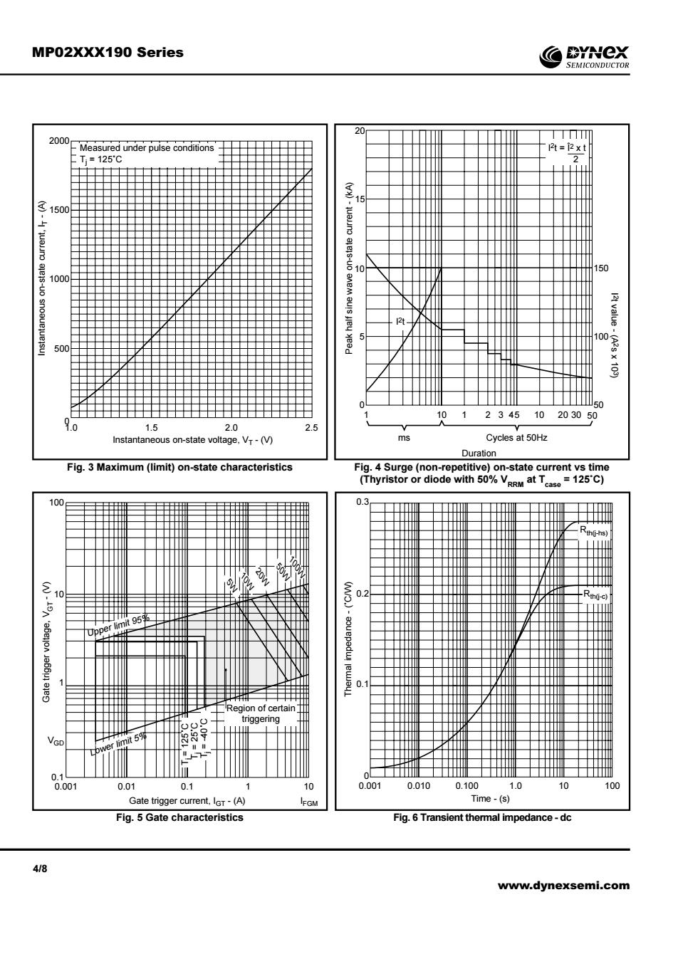
MP02XXX190 Series BYNeX ONDUCTO 108 234510203050 20 Cycles at 50H Maximum (lim aracteristics of ate trigg Time -(s) GM Fig.5 G ig.thermal impedance .dc www.dynexsemi.com
4/8 www.dynexsemi.com MP02XXX190 Series 1.0 1.5 2.0 2.5 Instantaneous on-state voltage, VT - (V) 0 500 1000 1500 2000 Instantaneous on-state current, IT - (A) Measured under pulse conditions Tj = 125˚C Fig. 6 Transient thermal impedance - dc Fig. 3 Maximum (limit) on-state characteristics Fig. 4 Surge (non-repetitive) on-state current vs time (Thyristor or diode with 50% VRRM at Tcase = 125˚C) Fig. 5 Gate characteristics 0.001 0.010 0.100 1.0 10 100 Time - (s) 0 0.1 0.2 0.3 Thermal impedance - (˚C/W) Rth(j-hs) Rth(j-c) 0.001 0.01 0.1 1 10 Gate trigger current, IGT - (A) 100 10 1 0.1 Gate trigger voltage, VGT - (V) 100W 50W 10W 20W 5W Region of certain triggering Upper limit 95% Lower limit 5% Tj = 125˚C Tj = 25˚C Tj = -40˚C VGD IFGM 20 15 10 5 0 Peak half sine wave on-state current - (kA) 1 10 1 2 3 45 50 ms Cycles at 50Hz Duration 50 100 I2t value - (A2s x 103) I2t I 2t = Î2 x t 2 150 10 20 30
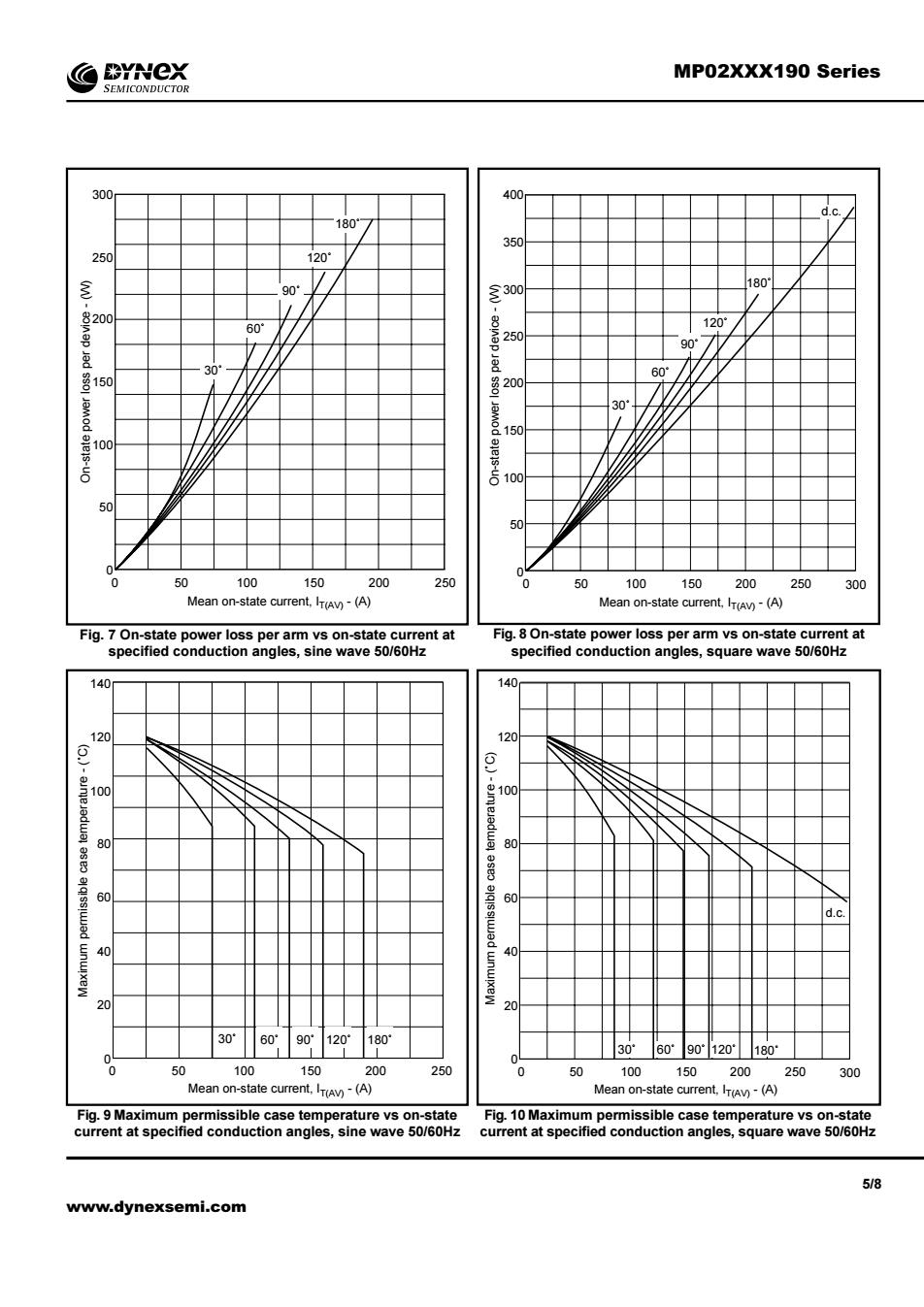
PYNeX MP02XXX190 Series 120 330 20 90° 150 50 Fig.7 On-s 6090120°180° 30 60 90120*180* te current,(A 50 Mean on 0 Fig.9 Ma 5/8 www.dynexsemi.com
5/8 www.dynexsemi.com MP02XXX190 Series Fig. 7 On-state power loss per arm vs on-state current at specified conduction angles, sine wave 50/60Hz Fig. 8 On-state power loss per arm vs on-state current at specified conduction angles, square wave 50/60Hz Fig. 9 Maximum permissible case temperature vs on-state current at specified conduction angles, sine wave 50/60Hz Fig. 10 Maximum permissible case temperature vs on-state current at specified conduction angles, square wave 50/60Hz 0 50 100 150 200 250 Mean on-state current, IT(AV) - (A) 300 250 200 150 100 50 0 On-state power loss per device - (W) 180˚ 120˚ 90˚ 60˚ 30˚ 0 50 100 150 200 250 300 Mean on-state current, IT(AV) - (A) 400 350 300 250 200 150 100 50 0 On-state power loss per device - (W) 180˚ 120˚ 90˚ 60˚ 30˚ d.c. 0 50 100 150 200 250 Mean on-state current, IT(AV) - (A) 120 100 80 60 40 20 0 Maximum permissible case temperature - (˚C) 30˚ 60˚ 90˚ 120˚ 180˚ 140 0 50 100 150 200 250 300 Mean on-state current, IT(AV) - (A) 120 100 80 60 40 20 0 Maximum permissible case temperature - (˚C) 30˚ 60˚ 90˚ 120˚ 180˚ 140 d.c