UQSTC 的 956 Modeling and Simulation in Epitaxial Growth
Modeling and Simulation in Epitaxial Growth
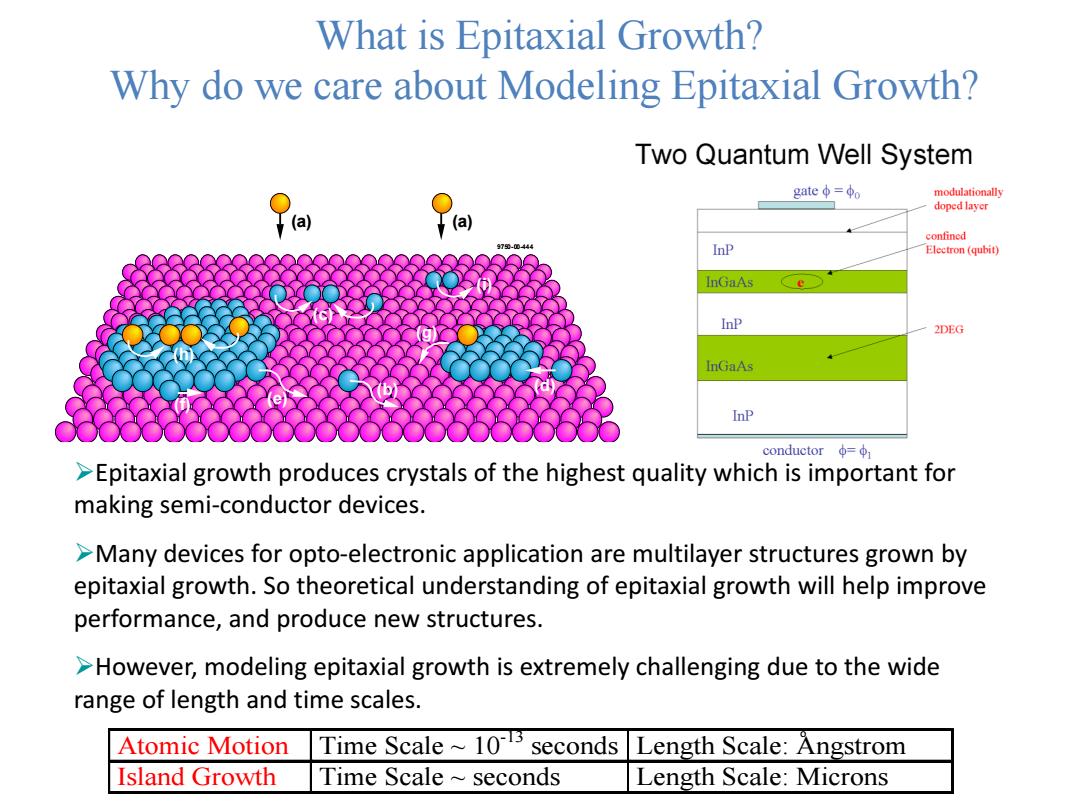
What is Epitaxial Growth? Why do we care about Modeling Epitaxial Growth? Two Quantum Well System gateφ=φo modulationally doped layer (a (a) confined 70-00444 InP Electron(qubit) InGaAs InP 2DEG InGaAs InP conductor=φ1 >Epitaxial growth produces crystals of the highest quality which is important for making semi-conductor devices. >Many devices for opto-electronic application are multilayer structures grown by epitaxial growth.So theoretical understanding of epitaxial growth will help improve performance,and produce new structures. >However,modeling epitaxial growth is extremely challenging due to the wide range of length and time scales. Atomic Motion Time Scale~103 seconds Length Scale:Angstrom Island Growth Time Scale seconds Length Scale:Microns
9750-00-444 (a) (a) (h) (f) (e) (b) (c) (i) (g) (d) What is Epitaxial Growth? Why do we care about Modeling Epitaxial Growth? Atomic Motion Time Scale ~ 10-13 seconds Length Scale: Angstrom Island Growth Time Scale ~ seconds Length Scale: Microns o ➢Epitaxial growth produces crystals of the highest quality which is important for making semi-conductor devices. ➢Many devices for opto-electronic application are multilayer structures grown by epitaxial growth. So theoretical understanding of epitaxial growth will help improve performance, and produce new structures. ➢However, modeling epitaxial growth is extremely challenging due to the wide range of length and time scales
Modeling of Thin Film Growth >Mean-field Rate Equations: Easy to formulate and easy to solve. Contain no spatial information.Do not readily yield information on surface morphology. >Continuum Models:Completely deterministic method. Appropriate mainly at large time and length scales. Lack detail. >KMC simulations:Completely stochastic method. Very useful for identifying relevant microscopic processes. The time and size limitations make them unfeasible for studying epitaxial growth Detailed KMC simulations are extremely slow and expensive
Modeling of Thin Film Growth ➢Mean-field Rate Equations: ✓Easy to formulate and easy to solve. ❖Contain no spatial information. Do not readily yield information on surface morphology. ➢ Continuum Models: Completely deterministic method. ✓Appropriate mainly at large time and length scales. ❖Lack detail. ➢KMC simulations: Completely stochastic method. ✓Very useful for identifying relevant microscopic processes. ❖The time and size limitations make them unfeasible for studying epitaxial growth ❖Detailed KMC simulations are extremely slow and expensive
Smallest Metallic Nanorods Using Physical Vapor Deposition
Smallest Metallic Nanorods Using Physical Vapor Deposition
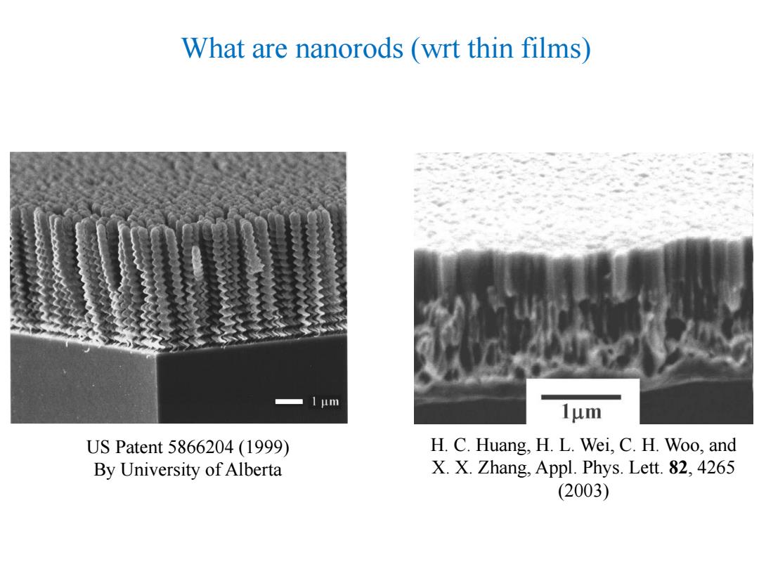
What are nanorods (wrt thin films) 1μm 1μm US Patent5866204(1999) H.C.Huang,H.L.Wei,C.H.Woo,and By University of Alberta X.X.Zhang,Appl.Phys.Lett.82,4265 (2003)
What are nanorods (wrt thin films) US Patent 5866204 (1999) By University of Alberta H. C. Huang, H. L. Wei, C. H. Woo, and X. X. Zhang, Appl. Phys. Lett. 82, 4265 (2003)