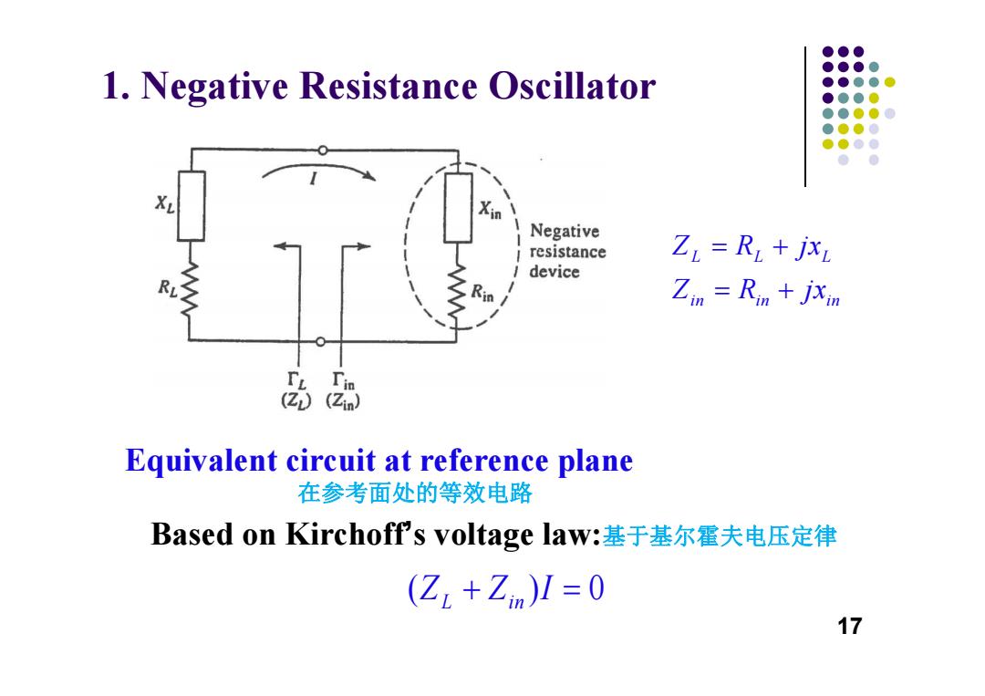
●●】 ●●●● 1.Negative Resistance Oscillator ●●●● ●●●● ●●●● ●●●● ●●●● ● Negative resistance Z=R+jxL device Zin Rin jxin 话 Equivalent circuit at reference plane 在参考面处的等效电路 Based on Kirchoff's voltage law:基于基尔霍夫电压定律 (Z,+Zn)M=0 17
1. Negative Resistance Oscillator in in in L L L Z R jx Z R jx Based on Kirchoff’s voltage law:基于基尔霍夫电压定律 ( Z Z ) I 0 L in Equivalent circuit at reference plane 在参考面处的等效电路 17
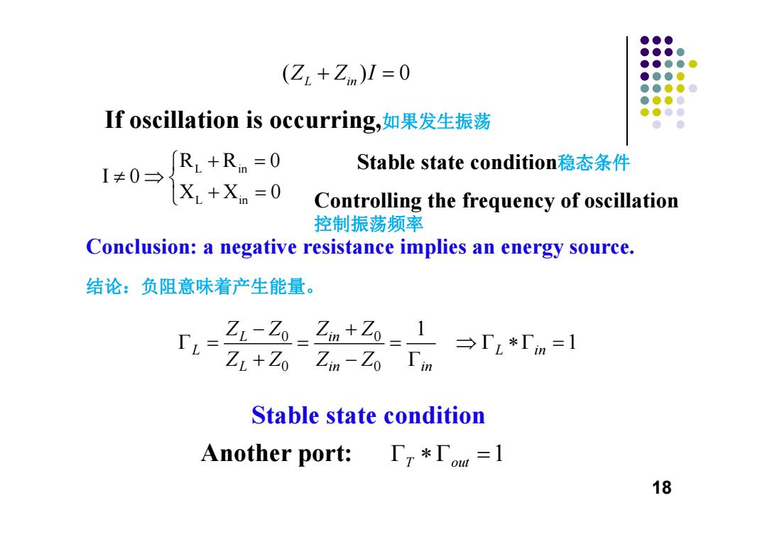
●●● ●●●● (Z,+Zn)1=0 ●●●●● ●●●0 ●●●● ●●●0 If oscillation is0 ccurring,如果发生振荡 ●●●● ● RL+Rin=0 Stable state condition稳态条件 I≠0→ X+Xin=0 Controlling the frequency of oscillation 控制振荡频率 Conclusion:a negative resistance implies an energy source. 结论:负阻意味着产生能量。 TL= -乙_乙m+Z=1→「L*「m= ZL+ZoZn-Z0「m Stable state condition Another port:I*To=1 18
Conclusion: a negative resistance implies an energy source. 结论:负阻意味着产生能量。 Stable state condition Another port: If oscillation is occurring,如果发生振荡 Stable state condition稳态条件 Controlling the frequency of oscillation 控制振荡频率 18 ( )0 Z ZI L in L in L in RR 0 I 0 XX 0 0 0 0 0 1 1 L in L L in L in in ZZ ZZ ZZ ZZ 1 T out
●●● ●●●● ●●●● Oscillation: ●●●● ●●●● ●●●0 ●●●● 1 Initially the overall circuit is unstable at a certain frequency. 最初,整个电路在某个频率上不稳定。 2The any transient excitation,such as noise or the turning on of the power supply,causes an oscillation at o. 任何一个瞬态激励,比如噪声或者加电,引起一个振荡 ③AsI↑,Rin must become less negative until I,is reached on Z(Lo)+Z=0.随着电流增加负阻变成负得不厉害,直到达到10 Then the oscillator will be running in a stable state. In practice:o≠oo OX i R=X4=-X al start up oscillation condition 19
① Initially the overall circuit is unstable at a certain frequency. 最初,整个电路在某个频率上不稳定。 ② The any transient excitation, such as noise or the turning on of the power supply, causes an oscillation at ω. 任何一个瞬态激励,比如噪声或者加电,引起一个振荡 ③ As I↑, Rin must become less negative until I0 is reached on Zin (I0)+ZL=0.随着电流增加负阻变成负得不厉害,直到达到I0 Oscillation: Then the oscillator will be running in a stable state. 0 I ω≠ω Xin 0 , 3 in L L in R R X X In practice: start up oscillation condition 19
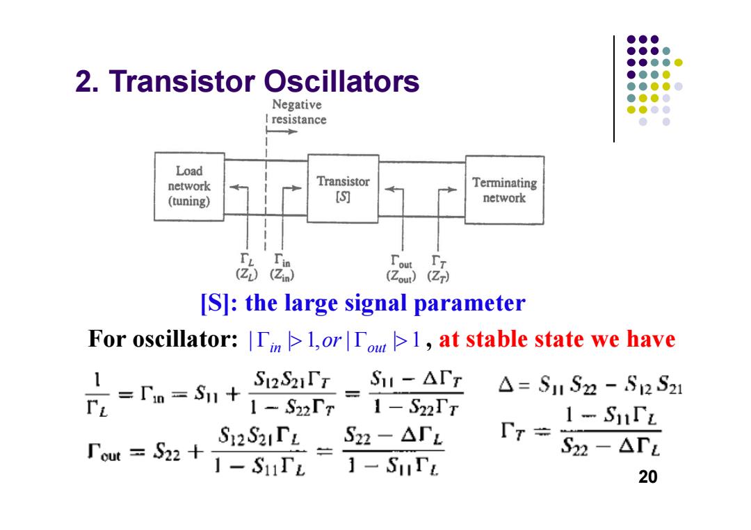
●●● ●●●● ●●●●● 2.Transistor Oscillators ●●●0 ●●●●0 ●●●● Negative ●●● Iresistance ● ● Load network Transistor Terminating (tuning) [) network TL Tin (Z(Z) (Zou)(Z) [S]:the large signal parameter For oscillator:,oro1,at stable state we have 1 S12S2TrSI-△TT TL=En-Sn+15at △=S1S22-Si2S21 1-S22ΓT 1-ShTL S2S21TLS22-△「L TT= 厂oun=S2+1-S11TL S22-△TE 1-Sur 20
2. Transistor Oscillators [S]: the large signal parameter | | 1, | | 1 in out For oscillator: , or at stable state we have 20
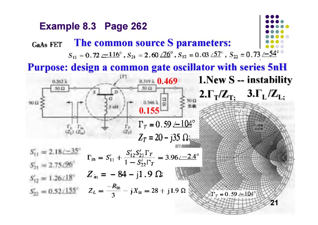
●●● ●●●● Example 8.3 Page 262 ●●●●● ●●●● ●●●●0 GaAs FET The common source S parameters: ●●●0 S=0.72-16°,S2=2.6076°,S2=0.0357,S2=0.73-54° Purpose:design a common gate oscillator with series 5nH 0.262入 0319x0.469 1.New S--instability 50a 500 2.「rZ3.「L/Z 0n3 0346入 50 0.155 品 Tx=0.59104° 2 Zr=20-j350 岳 51=2.18-35 Im =Si+ Si2STT =3.96-24° S31=2,7596 1-S22ΓT S2=1.2618 Zm=-84-j1.92 S=0.52155 2--j。-28+j19n Tx=0.59-1049 21
Example 8.3 Page 262 The common source S parameters: Purpose: design a common gate oscillator with series 5nH 1.New S -- instability 2.Γ T/ZT; 3.Γ L /ZL; 21 0.469 0.155