
Revision 2.0 Figure 5-15:Bulk Resistance Measurement..... .235 Figure 5-16.Test Structure for Impedance,Propagation Delay,and Crosstalk Measurements... .236 Figure 6-1:Configuration View of an A.G.P.Target................................ .244 Figure 6-2:Location of A.G.P.Capabilities............................... .247 Figure 6-3:PCI Device Block......... 252 Figure 6-4:A.G.P.Block.. 253 16
Revision 2.0 16 Figure 5-15: Bulk Resistance Measurement............................................................................................................. 235 Figure 5-16. Test Structure for Impedance, Propagation Delay, and Crosstalk Measurements................................ 236 Figure 6-1: Configuration View of an A.G.P. Target ............................................................................................... 244 Figure 6-2: Location of A.G.P. Capabilities............................................................................................................. 247 Figure 6-3: PCI Device Block .................................................................................................................................. 252 Figure 6-4: A.G.P. Block.......................................................................................................................................... 253
Revision 2.0 Tables Table 3-1:A.G.P.Requests .32 Table 3-2:A.G.P.Flow Control.................... 32 Table 3-3:A.G.P.Status Signals....... .33 Table 3-4:A.G.P.Clock List....... 34 Table 3-5:USB Signals.... .35 Table 3-6:Power Management on A.G.P. 35 Table 3-7:Special Interface Signals.................... 35 Table 3-8:PCI Signals in Relation to A.G.P..... .36 Table 3-9:Summary of Interfaces Based on Function and Agent... .37 Table 3-10:Summary of PCI Signals Based on Function and Agent. 38 Table 3-11:Summary of A.G.P.Signals Based on Function and Agent 39 Table 3-12:A.G.P.Bus Commands................................. 44 Table 3-13:SBA Port Encoding.......... 54 Table 3-14:SBA Signals. .55 Table 3-15:A.G.P.Master Flow Control Conditions. 62 Table 3-16:A.G.P.Target Flow Control Conditions..................... 63 Table 3-17:Data Buffering for 2x Transfers......... 65 Table 3-18:Data Buffering for 4x Transfers....... 66 Table 3-19:Back to Back Transactions............... .95 Table 3-20:A.G.P.Arbitration Rules........... .119 Table 3-21:Current/Next AD Activity............ 126 Table 4-1:Allowed Transfer Mode Signaling Levels....................... 156 Table 4-2:DC Specifications for A.G.P.1x Signaling at 3.3 Volts 165 Table 4-3:DC Specifications for A.G.P.Ix Signaling at 1.5 Volts................................ 165 Table 4-4:DC Specifications for 2x Mode only at 3.3 Volts Signaling.... 166 Table 4-5:DC Specifications for 2x or 4x Mode at 1.5 Volts Signaling....... 166 Table 4-6:A.G.P.1x AC Timing Parameters............................ 168 Table 4-7:A.G.P.2x AC Timing Parameters.............. .170 Table 4-8:A.G.P.4x AC Timing Parameters..... 172 Table 4-9:Measurement and Test Condition Parameters.......... 174 17
Revision 2.0 17 Tables Table 3-1: A.G.P. Requests ........................................................................................................................................ 32 Table 3-2: A.G.P. Flow Control ................................................................................................................................. 32 Table 3-3: A.G.P. Status Signals ................................................................................................................................ 33 Table 3-4: A.G.P. Clock List...................................................................................................................................... 34 Table 3-5: USB Signals .............................................................................................................................................. 35 Table 3-6: Power Management on A.G.P................................................................................................................... 35 Table 3-7: Special Interface Signals ........................................................................................................................... 35 Table 3-8: PCI Signals in Relation to A.G.P. ............................................................................................................. 36 Table 3-9: Summary of Interfaces Based on Function and Agent .............................................................................. 37 Table 3-10: Summary of PCI Signals Based on Function and Agent ......................................................................... 38 Table 3-11: Summary of A.G.P. Signals Based on Function and Agent .................................................................... 39 Table 3-12: A.G.P. Bus Commands ........................................................................................................................... 44 Table 3-13: SBA Port Encoding................................................................................................................................. 54 Table 3-14: SBA Signals ............................................................................................................................................ 55 Table 3-15: A.G.P. Master Flow Control Conditions ................................................................................................. 62 Table 3-16: A.G.P. Target Flow Control Conditions ................................................................................................. 63 Table 3-17: Data Buffering for 2x Transfers .............................................................................................................. 65 Table 3-18: Data Buffering for 4x Transfers .............................................................................................................. 66 Table 3-19: Back to Back Transactions...................................................................................................................... 95 Table 3-20: A.G.P. Arbitration Rules....................................................................................................................... 119 Table 3-21: Current/Next AD Activity..................................................................................................................... 126 Table 4-1: Allowed Transfer Mode Signaling Levels .............................................................................................. 156 Table 4-2: DC Specifications for A.G.P. 1x Signaling at 3.3 Volts ......................................................................... 165 Table 4-3: DC Specifications for A.G.P. 1x Signaling at 1.5 Volts ......................................................................... 165 Table 4-4: DC Specifications for 2x Mode only at 3.3 Volts Signaling ................................................................... 166 Table 4-5: DC Specifications for 2x or 4x Mode at 1.5 Volts Signaling .................................................................. 166 Table 4-6: A.G.P. 1x AC Timing Parameters........................................................................................................... 168 Table 4-7: A.G.P. 2x AC Timing Parameters........................................................................................................... 170 Table 4-8: A.G.P. 4x AC Timing Parameters........................................................................................................... 172 Table 4-9: Measurement and Test Condition Parameters ......................................................................................... 174
Revision 2.0 Table 4-10:Clock Skew Parameters,All Transfer Rates........ .179 Table 4-11:Motherboard/Add-in Card Interoperability.............. 185 Table 4-12:Pull-up/Pull-down Resistor Values................. 186 Table 4-13:Parameters for Maximum AC A.G.P.Signaling Waveforms.... 187 Table 4-14:Add-in Card Power Supply Limits............. 188 Table 4-15:Signal Integrity Requirements'........... 189 Table 4-16:AC Specifications for A.G.P.3.3 Volt Signaling. 192 Table 4-17:AC Specifications for A.G.P.1.5 Volt Signaling... 192 Table 4-18:1x/2x Mode System Timing Summary....... 193 Table 4-19:1x/2x Mode Interconnect Delay Summary.......... 194 Table 4-20:1x/2x Mode Motherboard Interconnect Delays 195 Table 4-21:1x/2x Mode Add-in Card Interconnect Delays........... 197 Table 4-22:A.G.P.4x Timing and Signal Integrity Requirements. 199 Table 4-23:AC Specifications for A.G.P.1.5 Volt Signaling..... 203 Table 4-24:4x Mode Add-in Card Source Synchronous Interconnect Summary. 207 Table 5-1:Thermal Specification for Add-in Cards........ 217 Table 5-2:A.G.P.Motherboard Connector Pinout... 231 Table 5-3:Qualification Test....... 241 Table 6-1:Commands Supported by Each Port. 246 Table 6-2:A.G.P.Options. 254 18
Revision 2.0 18 Table 4-10: Clock Skew Parameters, All Transfer Rates ......................................................................................... 179 Table 4-11: Motherboard / Add-in Card Interoperability ......................................................................................... 185 Table 4-12: Pull-up/Pull-down Resistor Values ....................................................................................................... 186 Table 4-13: Parameters for Maximum AC A.G.P. Signaling Waveforms................................................................ 187 Table 4-14: Add-in Card Power Supply Limits........................................................................................................ 188 Table 4-15: Signal Integrity Requirements1 .............................................................................................................. 189 Table 4-16: AC Specifications for A.G.P. 3.3 Volt Signaling.................................................................................. 192 Table 4-17: AC Specifications for A.G.P. 1.5 Volt Signaling.................................................................................. 192 Table 4-18: 1x / 2x Mode System Timing Summary................................................................................................ 193 Table 4-19: 1x / 2x Mode Interconnect Delay Summary.......................................................................................... 194 Table 4-20: 1x / 2x Mode Motherboard Interconnect Delays................................................................................... 195 Table 4-21: 1x / 2x Mode Add-in Card Interconnect Delays ................................................................................... 197 Table 4-22: A.G.P. 4x Timing and Signal Integrity Requirements........................................................................... 199 Table 4-23: AC Specifications for A.G.P. 1.5 Volt Signaling.................................................................................. 203 Table 4-24: 4x Mode Add-in Card Source Synchronous Interconnect Summary...................................................... 207 Table 5-1: Thermal Specification for Add-in Cards ................................................................................................. 217 Table 5-2: A.G.P. Motherboard Connector Pinout ................................................................................................... 231 Table 5-3: Qualification Test.................................................................................................................................... 241 Table 6-1: Commands Supported by Each Port........................................................................................................ 246 Table 6-2: A.G.P. Options........................................................................................................................................ 254
Revision 2.0 1.Introduction The Accelerated Graphics Port(AGP or A.G.P.)is a high performance,component level interconnect targeted at 3D graphical display applications.A.G.P.is based on a set of performance extensions or enhancements to the PCI bus. This document specifies the A.G.P.interface,and provides some design suggestions for effectively using it in high performance 3D graphics display applications. 1.1 Motivation In general,3D rendering has a voracious appetite for memory bandwidth,and continues to put upward pressure on memory footprint as well.As 3D hardware and software become more pervasive,these two trends are likely to accelerate,requiring high speed access to ever larger amounts of memory,thus raising the bill of material costs for 3D enabled platforms.Containing these costs while enabling performance improvements is the primary motivation for the A.G.P.By providing up to an order of magnitude bandwidth improvement between the graphics accelerator and system memory,some of the 3D rendering data structures may be effectively shifted into main memory,relieving the pressure to increase the cost of the local graphics memory Texture data are the first structures targeted for shifting to system memory for four reasons: 1.Textures are generally read only,and,therefore,do not have special access ordering or coherency problems. 2.Shifting textures balances the bandwidth load between system memory and local graphics memory,since a well cached host processor has much lower memory bandwidth requirements than does a 3D rendering engine. Texture access comprises perhaps the largest single component of rendering memory bandwidth(compared with rendering,display and Z buffers):so avoiding loading or caching textures in graphics local memory saves not only this component of local memory bandwidth,but also the bandwidth necessary to load the texture store in the first place.Furthermore,this data must pass through main memory anyway as it is loaded from a mass store device 3. Texture size is dependent upon application quality rather than on display resolution,and,therefore,subject to the greatest pressure for growth 4. Texture data is not persistent,it resides in memory only for the duration of the application,so any system memory spent on texture storage can be returned to the free memory heap when the application concludes (unlike display buffers which remain in persistent use). Other data structures may be moved to main memory but texture data is the biggest win. Reducing costs by moving graphics data to main memory is the primary motivation for the A.G.P.,which is designed to provide a smooth,incremental transition for today's PCI based graphics vendors as they develop higher performance components in the future. 19
Revision 2.0 19 The Accelerated Graphics Port (AGP or A.G.P.) is a high performance, component level interconnect targeted at 3D graphical display applications. A.G.P. is based on a set of performance extensions or enhancements to the PCI bus. This document specifies the A.G.P. interface, and provides some design suggestions for effectively using it in high performance 3D graphics display applications. 1.1 Motivation In general, 3D rendering has a voracious appetite for memory bandwidth, and continues to put upward pressure on memory footprint as well. As 3D hardware and software become more pervasive, these two trends are likely to accelerate, requiring high speed access to ever larger amounts of memory, thus raising the bill of material costs for 3D enabled platforms. Containing these costs while enabling performance improvements is the primary motivation for the A.G.P. By providing up to an order of magnitude bandwidth improvement between the graphics accelerator and system memory, some of the 3D rendering data structures may be effectively shifted into main memory, relieving the pressure to increase the cost of the local graphics memory. Texture data are the first structures targeted for shifting to system memory for four reasons: 1. Textures are generally read only, and, therefore, do not have special access ordering or coherency problems. 2. Shifting textures balances the bandwidth load between system memory and local graphics memory, since a well cached host processor has much lower memory bandwidth requirements than does a 3D rendering engine. Texture access comprises perhaps the largest single component of rendering memory bandwidth (compared with rendering, display and Z buffers): so avoiding loading or caching textures in graphics local memory saves not only this component of local memory bandwidth, but also the bandwidth necessary to load the texture store in the first place. Furthermore, this data must pass through main memory anyway as it is loaded from a mass store device. 3. Texture size is dependent upon application quality rather than on display resolution, and, therefore, subject to the greatest pressure for growth. 4. Texture data is not persistent; it resides in memory only for the duration of the application, so any system memory spent on texture storage can be returned to the free memory heap when the application concludes (unlike display buffers which remain in persistent use). Other data structures may be moved to main memory but texture data is the biggest win. Reducing costs by moving graphics data to main memory is the primary motivation for the A.G.P., which is designed to provide a smooth, incremental transition for today’s PCI based graphics vendors as they develop higher performance components in the future. 1. Introduction
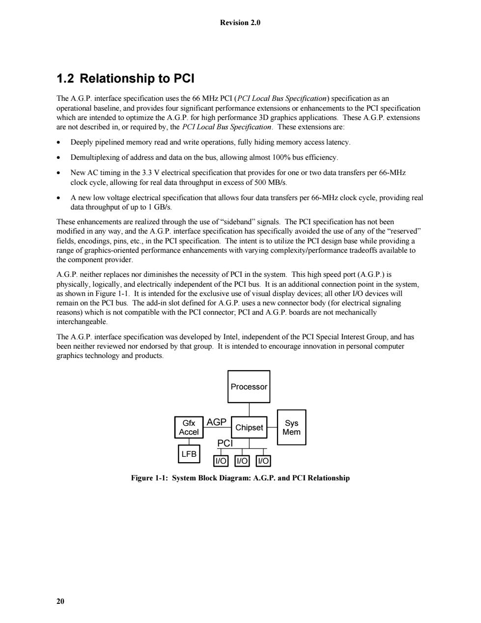
Revision 2.0 1.2 Relationship to PCI The A.G.P.interface specification uses the 66 MHz PCI (PCI Local Bus Specification)specification as an operational baseline,and provides four significant performance extensions or enhancements to the PCI specification which are intended to optimize the A.G.P.for high performance 3D graphics applications.These A.G.P.extensions are not described in,or required by,the PCI Local Bus Specification.These extensions are: Deeply pipelined memory read and write operations,fully hiding memory access latency. Demultiplexing of address and data on the bus,allowing almost 100%bus efficiency. New AC timing in the 3.3 V electrical specification that provides for one or two data transfers per 66-MHz clock cycle,allowing for real data throughput in excess of 500 MB/s. A new low voltage electrical specification that allows four data transfers per 66-MHz clock cycle,providing real data throughput of up to 1 GB/s. These enhancements are realized through the use of"sideband"signals.The PCI specification has not been modified in any way,and the A.G.P.interface specification has specifically avoided the use of any of the "reserved" fields,encodings,pins,etc.,in the PCI specification.The intent is to utilize the PCI design base while providing a range of graphics-oriented performance enhancements with varying complexity/performance tradeoffs available to the component provider. A.G.P.neither replaces nor diminishes the necessity of PCI in the system.This high speed port(A.G.P.)is physically,logically,and electrically independent of the PCI bus.It is an additional connection point in the system, as shown in Figure 1-1.It is intended for the exclusive use of visual display devices;all other I/O devices will remain on the PCI bus.The add-in slot defined for A.G.P.uses a new connector body (for electrical signaling reasons)which is not compatible with the PCI connector;PCI and A.G.P.boards are not mechanically interchangeable. The A.G.P.interface specification was developed by Intel,independent of the PCI Special Interest Group,and has been neither reviewed nor endorsed by that group.It is intended to encourage innovation in personal computer graphics technology and products. Processor Gfx AGP Chipset Sys Accel Mem PCI LFB 问问回 Figure 1-1:System Block Diagram:A.G.P.and PCI Relationship 20
Revision 2.0 20 1.2 Relationship to PCI The A.G.P. interface specification uses the 66 MHz PCI (PCI Local Bus Specification) specification as an operational baseline, and provides four significant performance extensions or enhancements to the PCI specification which are intended to optimize the A.G.P. for high performance 3D graphics applications. These A.G.P. extensions are not described in, or required by, the PCI Local Bus Specification. These extensions are: • Deeply pipelined memory read and write operations, fully hiding memory access latency. • Demultiplexing of address and data on the bus, allowing almost 100% bus efficiency. • New AC timing in the 3.3 V electrical specification that provides for one or two data transfers per 66-MHz clock cycle, allowing for real data throughput in excess of 500 MB/s. • A new low voltage electrical specification that allows four data transfers per 66-MHz clock cycle, providing real data throughput of up to 1 GB/s. These enhancements are realized through the use of “sideband” signals. The PCI specification has not been modified in any way, and the A.G.P. interface specification has specifically avoided the use of any of the “reserved” fields, encodings, pins, etc., in the PCI specification. The intent is to utilize the PCI design base while providing a range of graphics-oriented performance enhancements with varying complexity/performance tradeoffs available to the component provider. A.G.P. neither replaces nor diminishes the necessity of PCI in the system. This high speed port (A.G.P.) is physically, logically, and electrically independent of the PCI bus. It is an additional connection point in the system, as shown in Figure 1-1. It is intended for the exclusive use of visual display devices; all other I/O devices will remain on the PCI bus. The add-in slot defined for A.G.P. uses a new connector body (for electrical signaling reasons) which is not compatible with the PCI connector; PCI and A.G.P. boards are not mechanically interchangeable. The A.G.P. interface specification was developed by Intel, independent of the PCI Special Interest Group, and has been neither reviewed nor endorsed by that group. It is intended to encourage innovation in personal computer graphics technology and products. Processor LFB Gfx Accel Chipset Sys Mem I/O I/O I/O AGP PCI Figure 1-1: System Block Diagram: A.G.P. and PCI Relationship