Revision 2.0 Figures Figure 1-1:System Block Diagram:A.G.P.and PCI Relationship .20 Figure 2-1:Graphics Address Remapping Function....... .24 Figure 2-2:A.G.P.Access Queuing Model................. 25 Figure 2-3:Different Corelogic Architectures............. 27 Figure 3-1:Basic A.G.P.Pipeline Concept..... 42 Figure 3-2:A.G.P./PCI Operational States. 42 Figure 3-3:Layout of an A.G.P.Access Request 44 Figure 3-4:A.G.P.Request.. 53 Figure 3-5:SBA Port Request-1x...... 56 Figure 3-6:1x Sideband Addressing 56 Figure 3-7:2x Sideband Addressing............... 57 Figure 3-8:4x Sideband Addressing 57 Figure 3-9:Single Address................. 58 Figure 3-10:Multiple Addresses Enqueued,Maximum Delay by Master.... .58 Figure 3-11:Single 64-bit Request............ 59 Figure 3-12:Multiple 64-bit Requests. 60 Figure 3-13:32-bit and 64-bit Requests....... 60 Figure 3-14:Maximum Number of GNT#s Queued Before the Assertion of RBF# 67 Figure 3-15:Read Transaction with TP with No Waitstate......... 68 Figure 3-16:Read Transaction with TP with a Waitstate............... 68 Figure 3-17:Write Transaction with TP with No Waitstate..... 69 Figure 3-18:Write Transaction with TP with a Waitstate.................. 69 Figure 3-19:Maximum Delay by Master on Write Data............... 70 Figure 3-20:Write Data with One Tp 个 Figure 3-21:Minimum Delay by Target of Read Transaction...... 72 Figure 3-22:Minimum Delay on Back-to-Back Read Data............ 73 Figure 3-23:Master Does Not Delay Providing Write Data........... 74 Figure 3-24:Back-to-Back Write Data Transfers-No Delay.............. .75 Figure 3-25:2x Read Data-No Delay.... 76 Figure 3-26:2x Back-to-Back Read Data-No Delay...................... .76 11
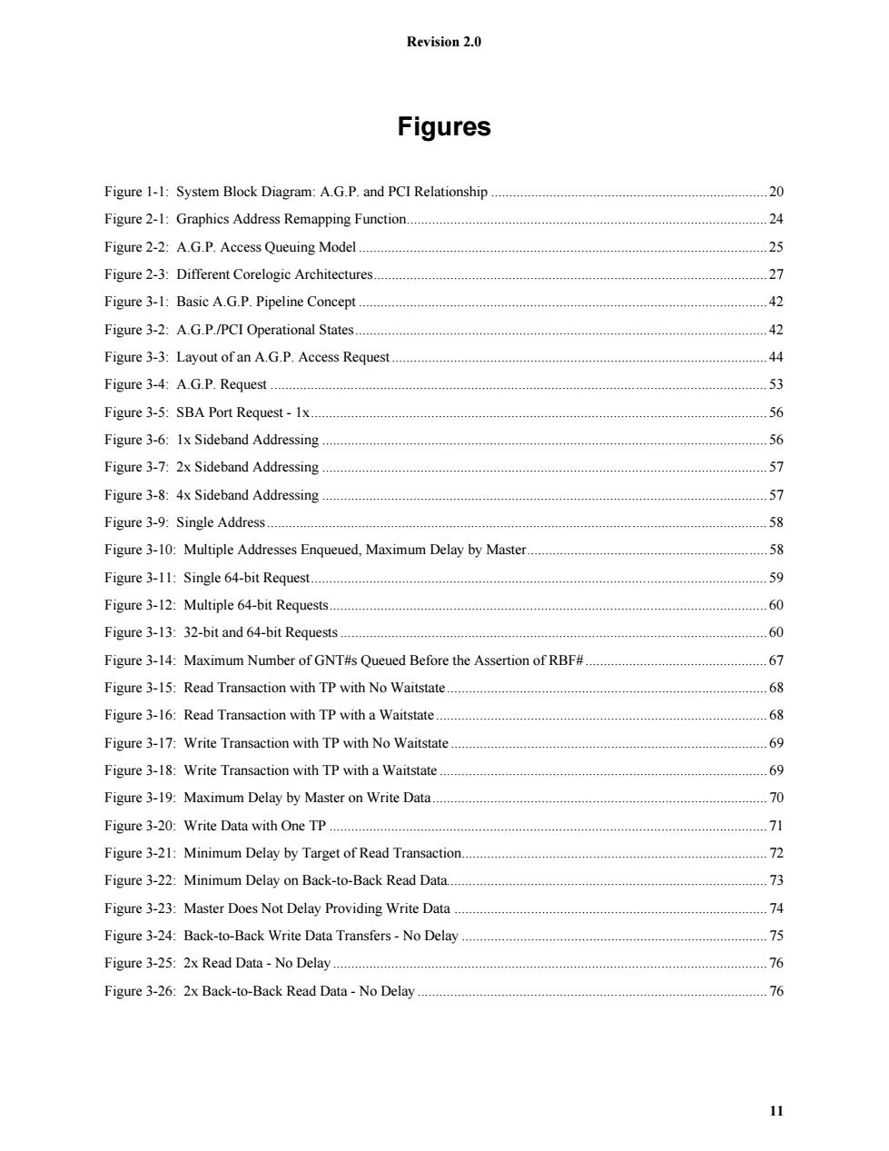
Revision 2.0 11 Figures Figure 1-1: System Block Diagram: A.G.P. and PCI Relationship ............................................................................ 20 Figure 2-1: Graphics Address Remapping Function................................................................................................... 24 Figure 2-2: A.G.P. Access Queuing Model ................................................................................................................ 25 Figure 2-3: Different Corelogic Architectures............................................................................................................ 27 Figure 3-1: Basic A.G.P. Pipeline Concept ................................................................................................................ 42 Figure 3-2: A.G.P./PCI Operational States................................................................................................................. 42 Figure 3-3: Layout of an A.G.P. Access Request ....................................................................................................... 44 Figure 3-4: A.G.P. Request ........................................................................................................................................ 53 Figure 3-5: SBA Port Request - 1x............................................................................................................................. 56 Figure 3-6: 1x Sideband Addressing .......................................................................................................................... 56 Figure 3-7: 2x Sideband Addressing .......................................................................................................................... 57 Figure 3-8: 4x Sideband Addressing .......................................................................................................................... 57 Figure 3-9: Single Address ......................................................................................................................................... 58 Figure 3-10: Multiple Addresses Enqueued, Maximum Delay by Master.................................................................. 58 Figure 3-11: Single 64-bit Request............................................................................................................................. 59 Figure 3-12: Multiple 64-bit Requests........................................................................................................................ 60 Figure 3-13: 32-bit and 64-bit Requests ..................................................................................................................... 60 Figure 3-14: Maximum Number of GNT#s Queued Before the Assertion of RBF# .................................................. 67 Figure 3-15: Read Transaction with TP with No Waitstate........................................................................................ 68 Figure 3-16: Read Transaction with TP with a Waitstate ........................................................................................... 68 Figure 3-17: Write Transaction with TP with No Waitstate ....................................................................................... 69 Figure 3-18: Write Transaction with TP with a Waitstate .......................................................................................... 69 Figure 3-19: Maximum Delay by Master on Write Data............................................................................................ 70 Figure 3-20: Write Data with One TP ........................................................................................................................ 71 Figure 3-21: Minimum Delay by Target of Read Transaction.................................................................................... 72 Figure 3-22: Minimum Delay on Back-to-Back Read Data........................................................................................ 73 Figure 3-23: Master Does Not Delay Providing Write Data ...................................................................................... 74 Figure 3-24: Back-to-Back Write Data Transfers - No Delay .................................................................................... 75 Figure 3-25: 2x Read Data - No Delay ....................................................................................................................... 76 Figure 3-26: 2x Back-to-Back Read Data - No Delay ................................................................................................ 76

Revision 2.0 Figure 3-27:2x Basic Write-No Delay........... .77 Figure 3-28:QuadWord Writes Back-to-Back-No Delay..... 77 Figure 3-29:Maximum Shift Between xRDY#and AD_STBx 78 Figure 3-30:Minimum Shift Between xRDY#and AD_STBx 79 Figure 3-31:4x Read Data-No Delay.... 80 Figure 3-32:4x Back-to-Back Read Data-No Delay..... 81 Figure 3-33:4x Basic Write-No Delay.......... 82 Figure 3-34:4x QuadWord Writes-No Delay.... 83 Figure 3-35:Minimum Delay for AD_STBx. 85 Figure 3-36:Maximum Delay for AD_STBx....... .86 Figure 3-37:Transaction with Subsequent Block. 87 Figure 3-38:Master Delays Data One Clock........... 88 Figure 3-39:Target Delays Subsequent Block.... 88 Figure 3-40:Target Stops Transaction After Second Block..... 89 Figure 3-41:Target Delays and Then Stops Transaction After Second Block. 90 Figure 3-42:Target Stop Transaction After First Block............. 9 Figure 3-43:Target Delays and Then Stops Transaction After First Block 92 Figure 3-44 Target-Abort 93 Figure 3-45:Master-Abort. 94 Figure 3-46:Back-to-Back Transaction with Turn-around Cycle... 96 Figure 3-47:Fast Back-to-Back Transaction. 97 Figure 3-48:WBF#Asserted Prevents Second Transaction......... 98 Figure 3-49:Second Transaction Prevented Because WBF#is Asserted. 99 Figure 3-50:Relationship of DEVSEL#and Short Transaction...... 100 Figure 3-51:Suppression of DEVSEL#on a Short Transaction.... 101 Figure 3-52:WBF#Asserted When First Transaction is Short....... 101 Figure 3-53:Back-to-Back Transaction When First Transaction is Short... 102 Figure 3-54:FW Followed by PCI Read by Corelogic.................. 103 Figure 3-55:PCI Read by Corelogic Followed by FW 104 Figure 3-56:FW Followed by an A.G.P.Read Data............ 105 Figure 3-57:Two Dead Clocks Between FW and an A.G.P.Read Data. 106 Figure 3-58:Short FW Followed by an A.G.P.Read Data...... 107 Figure 3-59:A.G.P.Read Followed by an FW Transaction................. .108 12
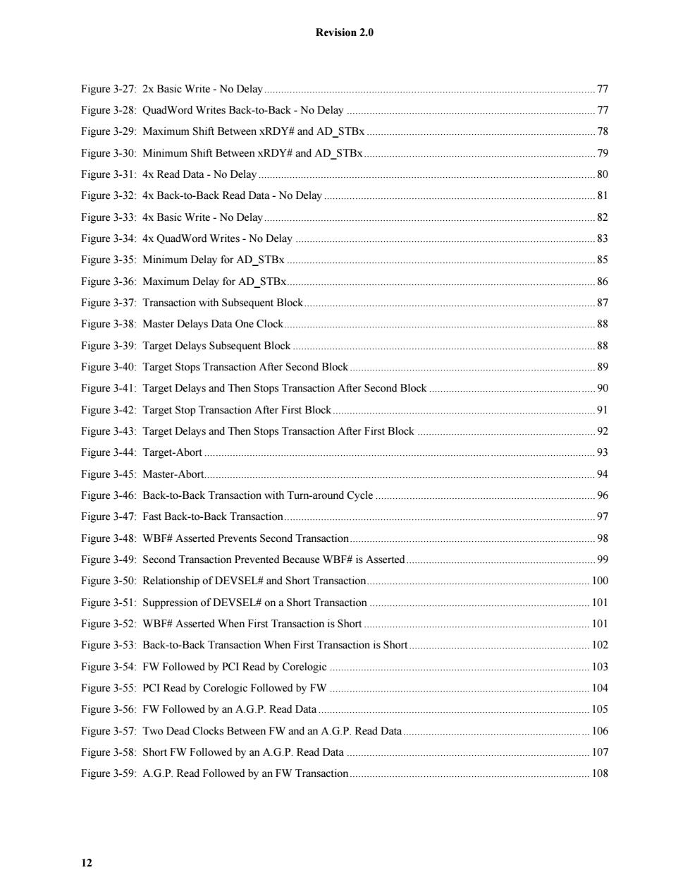
Revision 2.0 12 Figure 3-27: 2x Basic Write - No Delay..................................................................................................................... 77 Figure 3-28: QuadWord Writes Back-to-Back - No Delay ........................................................................................ 77 Figure 3-29: Maximum Shift Between xRDY# and AD_STBx ................................................................................. 78 Figure 3-30: Minimum Shift Between xRDY# and AD_STBx.................................................................................. 79 Figure 3-31: 4x Read Data - No Delay ....................................................................................................................... 80 Figure 3-32: 4x Back-to-Back Read Data - No Delay ................................................................................................ 81 Figure 3-33: 4x Basic Write - No Delay..................................................................................................................... 82 Figure 3-34: 4x QuadWord Writes - No Delay .......................................................................................................... 83 Figure 3-35: Minimum Delay for AD_STBx ............................................................................................................. 85 Figure 3-36: Maximum Delay for AD_STBx............................................................................................................. 86 Figure 3-37: Transaction with Subsequent Block....................................................................................................... 87 Figure 3-38: Master Delays Data One Clock.............................................................................................................. 88 Figure 3-39: Target Delays Subsequent Block ........................................................................................................... 88 Figure 3-40: Target Stops Transaction After Second Block....................................................................................... 89 Figure 3-41: Target Delays and Then Stops Transaction After Second Block ........................................................... 90 Figure 3-42: Target Stop Transaction After First Block............................................................................................. 91 Figure 3-43: Target Delays and Then Stops Transaction After First Block ............................................................... 92 Figure 3-44: Target-Abort .......................................................................................................................................... 93 Figure 3-45: Master-Abort.......................................................................................................................................... 94 Figure 3-46: Back-to-Back Transaction with Turn-around Cycle .............................................................................. 96 Figure 3-47: Fast Back-to-Back Transaction.............................................................................................................. 97 Figure 3-48: WBF# Asserted Prevents Second Transaction....................................................................................... 98 Figure 3-49: Second Transaction Prevented Because WBF# is Asserted................................................................... 99 Figure 3-50: Relationship of DEVSEL# and Short Transaction............................................................................... 100 Figure 3-51: Suppression of DEVSEL# on a Short Transaction .............................................................................. 101 Figure 3-52: WBF# Asserted When First Transaction is Short ................................................................................ 101 Figure 3-53: Back-to-Back Transaction When First Transaction is Short................................................................ 102 Figure 3-54: FW Followed by PCI Read by Corelogic ............................................................................................ 103 Figure 3-55: PCI Read by Corelogic Followed by FW ............................................................................................ 104 Figure 3-56: FW Followed by an A.G.P. Read Data ................................................................................................ 105 Figure 3-57: Two Dead Clocks Between FW and an A.G.P. Read Data.................................................................. 106 Figure 3-58: Short FW Followed by an A.G.P. Read Data ...................................................................................... 107 Figure 3-59: A.G.P. Read Followed by an FW Transaction..................................................................................... 108

Revision 2.0 Figure 3-60:FW Followed by an A.G.P.Write Data ..109 Figure 3-61:Long FW Followed by an A.G.P.Write Data...... 110 Figure 3-62:A.G.P.Write Followed by FW.................. .111 Figure 3-63:FW Followed by Graphics PCI Master Read...... .112 Figure 3-64:Graphics PCI Master Read Followed by FW. 113 Figure 3-65:FW Followed by Graphics PCI Master Write...... 114 Figure 3-66:Graphics PCI Master Write Followed by FW....... 115 Figure 3-67:FW Followed by an A.G.P.Request...... .116 Figure 3-68:Request Enqueued Followed by an FW Transaction 117 Figure 3-69:Request Followed by an FW Transaction............... 118 Figure 3-70:Single Address-No Delay by Master......... 120 Figure 3-71:Single Address-Maximum Delay by Master............. 121 Figure 3-72:PCI Write Transaction on the A.G.P.Interface.... 122 Figure 3-73:Arbiter Removes Grant-Master Does Not Start......... 123 Figure 3-74:Arbiter Removes Grant Later-Master Still Does Not Start.. 124 Figure 3-75:PIPE#Followed by an A.G.P.Master's PCI Read Transaction. 127 Figure 3-76:Double Phase PIPE#Followed by an A.G.P.Master PCI Write Transaction. 128 Figure 3-77:Back-to-Back PCI Read Transactions............................................ 129 Figure 3-78:Fast Back-to-Back PCI Write Transactions.............. 130 Figure 3-79:PCI Read Transaction Followed by PIPE#.... 131 Figure 3-80:PCI Write Transaction Followed by PIPE#......... 132 Figure 3-81:PIPE#Followed by Read Data............... 133 Figure 3-82:PIPE#Followed by Write Data....................... 133 Figure 3-83:Double Phase PIPE#Followed by Write Data....... 134 Figure 3-84:Master's PCI Read Transaction Followed by Read Data.... 135 Figure 3-85:A.G.P.Master's PCI Read Transaction Followed by Write Data. 136 Figure 3-86:A.G.P.Master's PCI Write Followed by Read Data.................. .137 Figure 3-87:Corelogic's PCI Write Followed by Read Data............... 137 Figure 3-88:Corelogic's PCI Write Transaction Followed by Write Data 138 Figure 3-89:A.G.P.Master's PCI Write Transaction Followed by Write Data 139 Figure 3-90:Single Read Data Followed by PIPE#.................. 140 Figure 3-91:Burst Read Data Followed by PIPE#......... .141 Figure 3-92:Single Write Data Followed by PIPE#..................... .142 13
Revision 2.0 13 Figure 3-60: FW Followed by an A.G.P. Write Data ............................................................................................... 109 Figure 3-61: Long FW Followed by an A.G.P. Write Data...................................................................................... 110 Figure 3-62: A.G.P. Write Followed by FW ............................................................................................................ 111 Figure 3-63: FW Followed by Graphics PCI Master Read....................................................................................... 112 Figure 3-64: Graphics PCI Master Read Followed by FW....................................................................................... 113 Figure 3-65: FW Followed by Graphics PCI Master Write...................................................................................... 114 Figure 3-66: Graphics PCI Master Write Followed by FW...................................................................................... 115 Figure 3-67: FW Followed by an A.G.P. Request.................................................................................................... 116 Figure 3-68: Request Enqueued Followed by an FW Transaction ........................................................................... 117 Figure 3-69: Request Followed by an FW Transaction ............................................................................................ 118 Figure 3-70: Single Address - No Delay by Master.................................................................................................. 120 Figure 3-71: Single Address - Maximum Delay by Master...................................................................................... 121 Figure 3-72: PCI Write Transaction on the A.G.P. Interface ................................................................................... 122 Figure 3-73: Arbiter Removes Grant - Master Does Not Start ................................................................................. 123 Figure 3-74: Arbiter Removes Grant Later - Master Still Does Not Start ................................................................ 124 Figure 3-75: PIPE# Followed by an A.G.P. Master’s PCI Read Transaction........................................................... 127 Figure 3-76: Double Phase PIPE# Followed by an A.G.P. Master PCI Write Transaction...................................... 128 Figure 3-77: Back-to-Back PCI Read Transactions.................................................................................................. 129 Figure 3-78: Fast Back-to-Back PCI Write Transactions ......................................................................................... 130 Figure 3-79: PCI Read Transaction Followed by PIPE# .......................................................................................... 131 Figure 3-80: PCI Write Transaction Followed by PIPE# ......................................................................................... 132 Figure 3-81: PIPE# Followed by Read Data ............................................................................................................ 133 Figure 3-82: PIPE# Followed by Write Data ........................................................................................................... 133 Figure 3-83: Double Phase PIPE# Followed by Write Data..................................................................................... 134 Figure 3-84: Master’s PCI Read Transaction Followed by Read Data..................................................................... 135 Figure 3-85: A.G.P. Master’s PCI Read Transaction Followed by Write Data ........................................................ 136 Figure 3-86: A.G.P. Master’s PCI Write Followed by Read Data............................................................................ 137 Figure 3-87: Corelogic’s PCI Write Followed by Read Data ................................................................................... 137 Figure 3-88: Corelogic’s PCI Write Transaction Followed by Write Data .............................................................. 138 Figure 3-89: A.G.P. Master's PCI Write Transaction Followed by Write Data........................................................ 139 Figure 3-90: Single Read Data Followed by PIPE# ................................................................................................. 140 Figure 3-91: Burst Read Data Followed by PIPE#................................................................................................... 141 Figure 3-92: Single Write Data Followed by PIPE# ................................................................................................ 142

Revision 2.0 Figure 3-93:Burst Write Data Followed by PIPE#...... .143 Figure 3-94:Single Read Data Followed by A.G.P.Master's PCI Transaction.............................1.43 Figure 3-95:Burst Read Data Followed by A.G.P.Corelogic's PCI Transaction. .144 Figure 3-96:Single Write Data Followed by AG.P.Master's PCI Transaction..............................1.45 Figure 3-97:Burst Write Data Followed by an A.G.P.Master's PCI Transaction. 146 Figure 3-98:Back-to-Back Read Data................... 147 Figure 3-99:GNT#Assertion for 16,8,and then 16 Byte Read Transfers..... 147 Figure 3-100:GNT#Assertion for Next Read Data After Long Data Transfer... .148 Figure 3-101:LP GNT#Pipelining Stopped While RBF#is Asserted..... 148 Figure 3-102:GNT#Assertion for Back-to-Back Write Data Transfers..... 149 Figure 3-103:Back-to-Back GNT#with Delay on Initial Transfer.. 150 Figure 3-104:Pipelined GNT#s-Read and Writes (Part 1)................ 151 Figure 3-105:Pipelined GNT#s-Read and Writes(Part 2). 151 Figure 3-106:A.G.P.Write Followed by a Read.......... 152 Figure 4-1:2x/4x Mode Time Domains............ 157 Figure 4-2:Mode Transmit Strobe/Data Timings................ 158 Figure 4-3:Receive Strobe/Data Timings..... 159 Figure 4-4:Transmit Strobe/Clock Timings............. 159 Figure 4-5:Composite 2x Mode Transmit Timings............. 160 Figure 4-6:Composite 4x Mode Transmit Timings........ 160 Figure 4-7:2x Mode Receiver Inner to Outer Loop Transfer Timing....... 161 Figure 4-8:4x Mode Receiver Inner to Outer Loop Transfer Timing.. 162 Figure 4-9:2x Composite Receive Timings............... 162 Figure 4-10:4x Composite Receive Timings..... 163 Figure 4-11:SB STB Synchronization Protocol. 164 Figure 4-12:A.G.P.1x Timing Diagram.......... 169 Figure 4-13:A.G.P.133 Timing Diagram.............. 171 Figure 4-14:Strobe/Data Turnaround Timings........ .171 Figure 4-15:4x Mode Timing Diagram..... 173 Figure 4-16:4x Mode Strobe/Data Turnaround Timings........ 173 Figure 4-17:Clock Input Measurement Conditions.... 174 Figure 4-18:Output Timing Measurement Conditions..... .175 Figure 4-19:Input Timing Measurement Conditions..................... .175 14
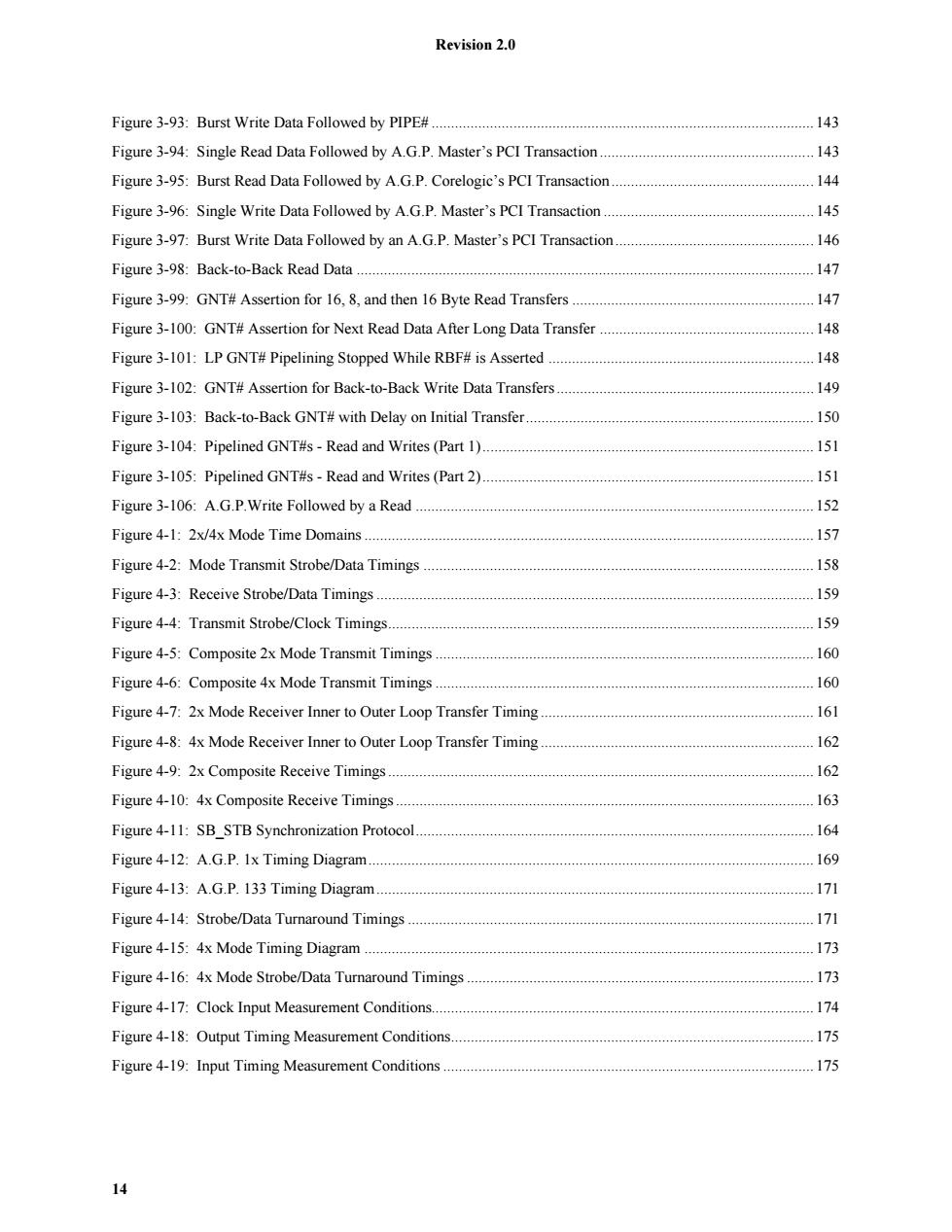
Revision 2.0 14 Figure 3-93: Burst Write Data Followed by PIPE# .................................................................................................. 143 Figure 3-94: Single Read Data Followed by A.G.P. Master’s PCI Transaction ....................................................... 143 Figure 3-95: Burst Read Data Followed by A.G.P. Corelogic’s PCI Transaction .................................................... 144 Figure 3-96: Single Write Data Followed by A.G.P. Master’s PCI Transaction ...................................................... 145 Figure 3-97: Burst Write Data Followed by an A.G.P. Master’s PCI Transaction ................................................... 146 Figure 3-98: Back-to-Back Read Data ..................................................................................................................... 147 Figure 3-99: GNT# Assertion for 16, 8, and then 16 Byte Read Transfers .............................................................. 147 Figure 3-100: GNT# Assertion for Next Read Data After Long Data Transfer ....................................................... 148 Figure 3-101: LP GNT# Pipelining Stopped While RBF# is Asserted .................................................................... 148 Figure 3-102: GNT# Assertion for Back-to-Back Write Data Transfers.................................................................. 149 Figure 3-103: Back-to-Back GNT# with Delay on Initial Transfer.......................................................................... 150 Figure 3-104: Pipelined GNT#s - Read and Writes (Part 1)..................................................................................... 151 Figure 3-105: Pipelined GNT#s - Read and Writes (Part 2)..................................................................................... 151 Figure 3-106: A.G.P.Write Followed by a Read ...................................................................................................... 152 Figure 4-1: 2x/4x Mode Time Domains ................................................................................................................... 157 Figure 4-2: Mode Transmit Strobe/Data Timings .................................................................................................... 158 Figure 4-3: Receive Strobe/Data Timings ................................................................................................................ 159 Figure 4-4: Transmit Strobe/Clock Timings............................................................................................................. 159 Figure 4-5: Composite 2x Mode Transmit Timings ................................................................................................. 160 Figure 4-6: Composite 4x Mode Transmit Timings ................................................................................................. 160 Figure 4-7: 2x Mode Receiver Inner to Outer Loop Transfer Timing ...................................................................... 161 Figure 4-8: 4x Mode Receiver Inner to Outer Loop Transfer Timing ...................................................................... 162 Figure 4-9: 2x Composite Receive Timings ............................................................................................................. 162 Figure 4-10: 4x Composite Receive Timings ........................................................................................................... 163 Figure 4-11: SB_STB Synchronization Protocol...................................................................................................... 164 Figure 4-12: A.G.P. 1x Timing Diagram.................................................................................................................. 169 Figure 4-13: A.G.P. 133 Timing Diagram................................................................................................................ 171 Figure 4-14: Strobe/Data Turnaround Timings ........................................................................................................ 171 Figure 4-15: 4x Mode Timing Diagram ................................................................................................................... 173 Figure 4-16: 4x Mode Strobe/Data Turnaround Timings ......................................................................................... 173 Figure 4-17: Clock Input Measurement Conditions.................................................................................................. 174 Figure 4-18: Output Timing Measurement Conditions............................................................................................. 175 Figure 4-19: Input Timing Measurement Conditions ............................................................................................... 175

Revision 2.0 Figure 4-20:Load for Testing Output Timings. .175 Figure 4-21:Flight Time and Skew Measurement. .176 Figure 4-22:4x Mode Buffer Test Load...... 177 Figure 4-23:4x Mode Delay Measurement Method.. .177 Figure 4-24:Methods of Measuring Slew Rate. 178 Figure 4-25:Clock Skew Diagram.......... 180 Figure 4-26:Source Generated Vref Scheme. 181 Figure 4-27:Recommended Component Pinout.... 183 Figure 4-28:Maximum AC Waveforms for A.G.P.Signaling 187 Figure 4-29:V/I Curves for 3.3 Volt Signaling............... 190 Figure 4-30:V/I Curves for 1.5 Volt Signaling 191 Figure 4-31:Flight Time. 200 Figure 4-32:Signal Integrity Conditions..... 200 Figure 4-33:V/I Curves for 1.5 Volt Signaling............. 202 Figure 4-34:Example of Routing Escaping a Component and Connector. 205 Figure 5-1A:3.3 Volt A.G.P.ATX Form Factor Add-in Card.... 210 Figure 5-1B:1.5 Volt A.G.P.ATX Form Factor Add-in Card 211 Figure 5-2:Detail A and B:A.G.P.Card Edge Finger Layout........ .212 Figure 5-3:A.G.P.NLX Form Factor Add-in Card................... 213 Figure 5-4:A.G.P.NLX Factor Add-in Card Comprehensive......... 214 Figure 5-5:A.G.P.NLX Form Factor Card Detail.. 215 Figure 5-6:A.G.P.NLX Form Factor Add-in Card Reference Bracket Details. 215 Figure 5-7:A.G.P.NLX Form Factor I/O Bracket and Chassis Interaction.... 216 Figure 5-8:A.G.P.Card Edge Connector Bevel........ 218 Figure 5-9A:A.G.P.3.3 Volt Connector Footprint and Layout Dimensions... 220 Figure 5-9B:A.G.P.3.3 Volt Connector Footprint and Layout Dimensions........... 221 Figure 5-10A:A.G.P.Universal Connector Footprint and Layout Dimensions.......................................... 223 Figure 5-10B:A.G.P.Universal Connector Footprint and Layout Dimensions.............. 224 Figure 5-11A:A.G.P.Add-in Card 1.5 Volt Connector Footprint and Layout Dimensions.... 226 Figure 5-11B:A.G.P.Add-in Card 1.5 Volt Connector Footprint and Layout Dimensions 227 Figure 5-12 Typical ATX 3.3 Volt Connector Implementation.... 228 Figure 5-13:Typical ATX Universal Connector Implementation..... 229 Figure 5-14:Typical ATX 1.5 Volt Connector Implementation................. 230 15
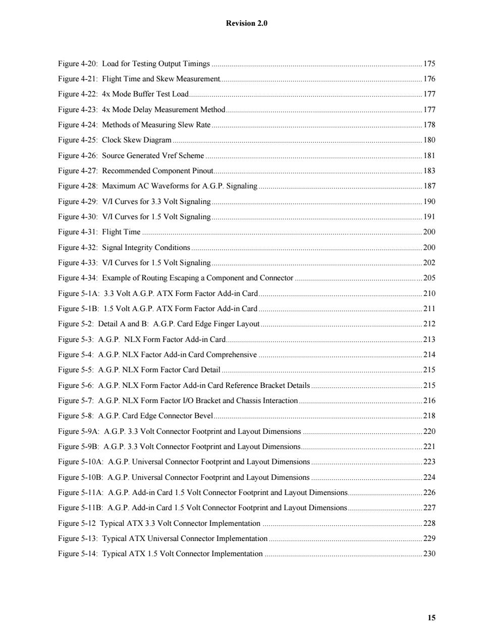
Revision 2.0 15 Figure 4-20: Load for Testing Output Timings ........................................................................................................ 175 Figure 4-21: Flight Time and Skew Measurement.................................................................................................... 176 Figure 4-22: 4x Mode Buffer Test Load................................................................................................................... 177 Figure 4-23: 4x Mode Delay Measurement Method................................................................................................. 177 Figure 4-24: Methods of Measuring Slew Rate........................................................................................................ 178 Figure 4-25: Clock Skew Diagram ........................................................................................................................... 180 Figure 4-26: Source Generated Vref Scheme ........................................................................................................... 181 Figure 4-27: Recommended Component Pinout....................................................................................................... 183 Figure 4-28: Maximum AC Waveforms for A.G.P. Signaling ................................................................................. 187 Figure 4-29: V/I Curves for 3.3 Volt Signaling........................................................................................................ 190 Figure 4-30: V/I Curves for 1.5 Volt Signaling........................................................................................................ 191 Figure 4-31: Flight Time .......................................................................................................................................... 200 Figure 4-32: Signal Integrity Conditions .................................................................................................................. 200 Figure 4-33: V/I Curves for 1.5 Volt Signaling........................................................................................................ 202 Figure 4-34: Example of Routing Escaping a Component and Connector ............................................................... 205 Figure 5-1A: 3.3 Volt A.G.P. ATX Form Factor Add-in Card................................................................................. 210 Figure 5-1B: 1.5 Volt A.G.P. ATX Form Factor Add-in Card................................................................................. 211 Figure 5-2: Detail A and B: A.G.P. Card Edge Finger Layout ................................................................................ 212 Figure 5-3: A.G.P. NLX Form Factor Add-in Card................................................................................................. 213 Figure 5-4: A.G.P. NLX Factor Add-in Card Comprehensive ................................................................................. 214 Figure 5-5: A.G.P. NLX Form Factor Card Detail ................................................................................................... 215 Figure 5-6: A.G.P. NLX Form Factor Add-in Card Reference Bracket Details ....................................................... 215 Figure 5-7: A.G.P. NLX Form Factor I/O Bracket and Chassis Interaction ............................................................. 216 Figure 5-8: A.G.P. Card Edge Connector Bevel....................................................................................................... 218 Figure 5-9A: A.G.P. 3.3 Volt Connector Footprint and Layout Dimensions ........................................................... 220 Figure 5-9B: A.G.P. 3.3 Volt Connector Footprint and Layout Dimensions............................................................ 221 Figure 5-10A: A.G.P. Universal Connector Footprint and Layout Dimensions ....................................................... 223 Figure 5-10B: A.G.P. Universal Connector Footprint and Layout Dimensions ....................................................... 224 Figure 5-11A: A.G.P. Add-in Card 1.5 Volt Connector Footprint and Layout Dimensions..................................... 226 Figure 5-11B: A.G.P. Add-in Card 1.5 Volt Connector Footprint and Layout Dimensions..................................... 227 Figure 5-12 Typical ATX 3.3 Volt Connector Implementation ............................................................................... 228 Figure 5-13: Typical ATX Universal Connector Implementation ............................................................................ 229 Figure 5-14: Typical ATX 1.5 Volt Connector Implementation .............................................................................. 230