
2.CMOS Process Step Step 2.Lithography sequence for n-well Photolithography:Transfer circuit layout information to the wafer Layout consists of polygons.Layout is first"written"to a transparant glass "mask"by a precisely controlled electron beam. Negative Photoresist(PR)deposition PR:A material whose etching properties change upon exposure to light.Negative PR "hardens"in regions exposed to UV light.Positive PR"hardens"in regions not exposed to UV light. Exposure to ultraviolet (UV)light using the n-well mask Selective etching.Etchant dissolves "soft"PR Photoresist p-substrate
2. CMOS Process Step Step 2. Lithography sequence for n-well • Photolithography: Transfer circuit layout information to the wafer Layout consists of polygons. Layout is first “written” to a transparant glass “mask” by a precisely controlled electron beam. • Negative Photoresist (PR) deposition PR: A material whose etching properties change upon exposure to light. Negative PR “hardens” in regions exposed to UV light. Positive PR “hardens” in regions not exposed to UV light. • Exposure to ultraviolet (UV) light using the n-well mask • Selective etching. Etchant dissolves “soft” PR

2.CMOS Process Step Step 3.Create n-wells through ion implantation n-wells required for p-channel devices n-channel devices will be fabricated directly in the native p-substrate lon implantation:Selectively introduce dopants into the wafer Doping atoms are accelerated as a high-energy focused beam,hitting the surface and penetrating the exposed areas.Doping level determined by intensity and duration of implantation. Retrograde profile:Peak of the doping concentration occurs well below the surface lon implantation n-type p-substrate
2. CMOS Process Step Step 3. Create n-wells through ion implantation • n-wells required for p-channel devices n-channel devices will be fabricated directly in the native p-substrate • Ion implantation: Selectively introduce dopants into the wafer Doping atoms are accelerated as a high-energy focused beam, hitting the surface and penetrating the exposed areas. Doping level determined by intensity and duration of implantation. Retrograde profile: Peak of the doping concentration occurs well below the surface

2.CMOS Process Step Step 4.Remove PR and oxide layer ●n-well completed Note:lon implantation damages the Si lattice Si lattice can be repaired through an annealing process.Annealing:Wafer is heated to 1000C for 15-30min allowing the lattice bonds to form again.Annealing causes dopant diffusion in all directions(e.g.side diffusion of S/D regions).Therefore,wafer is annealed only once after all implantations have been completed n-well p-substrate
2. CMOS Process Step Step 4. Remove PR and oxide layer • n-well completed • Note: Ion implantation damages the Si lattice Si lattice can be repaired through an annealing process. Annealing: Wafer is heated to 1000°C for 15-30min allowing the lattice bonds to form again. Annealing causes dopant diffusion in all directions (e.g. side diffusion of S/D regions). Therefore, wafer is annealed only once after all implantations have been completed
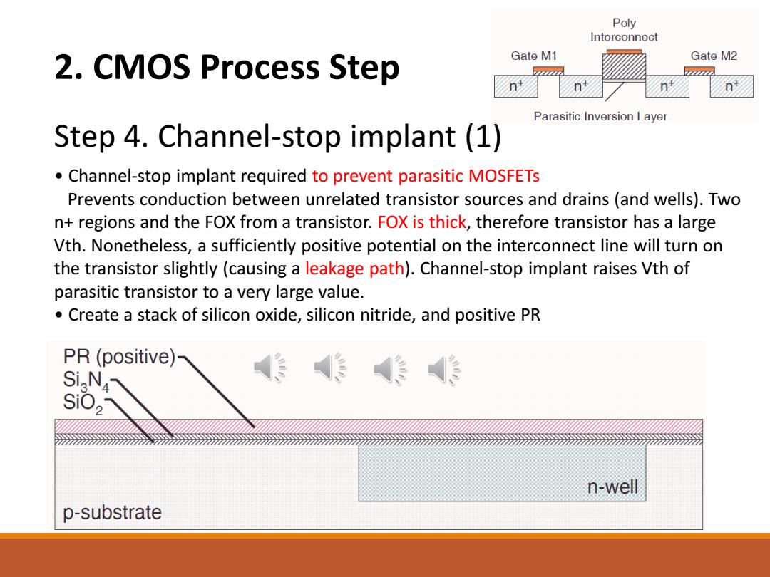
Poly Interconnect 2.CMOS Process Step Gate M1 Gate M2 224 Parasitic Inversion Layer Step 4.Channel-stop implant (1) Channel-stop implant required to prevent parasitic MOSFETs Prevents conduction between unrelated transistor sources and drains (and wells).Two n+regions and the FOX from a transistor.FOX is thick,therefore transistor has a large Vth.Nonetheless,a sufficiently positive potential on the interconnect line will turn on the transistor slightly(causing a leakage path).Channel-stop implant raises Vth of parasitic transistor to a very large value. Create a stack of silicon oxide,silicon nitride,and positive PR PR(positive)- Si N4 作 SiO, n-well p-substrate
2. CMOS Process Step Step 4. Channel-stop implant (1) • Channel-stop implant required to prevent parasitic MOSFETs Prevents conduction between unrelated transistor sources and drains (and wells). Two n+ regions and the FOX from a transistor. FOX is thick, therefore transistor has a large Vth. Nonetheless, a sufficiently positive potential on the interconnect line will turn on the transistor slightly (causing a leakage path). Channel-stop implant raises Vth of parasitic transistor to a very large value. • Create a stack of silicon oxide, silicon nitride, and positive PR

2.CMOS Process Step Step 4.Channel-stop implant (2) Lithography sequence for channel-stop implant(based on positive PR) Active or diffusion areas include the source/drain regions and the p+and n+openings for the substrate and well ties n-well p-substrate
2. CMOS Process Step Step 4. Channel-stop implant (2) • Lithography sequence for channel-stop implant (based on positive PR) Active or diffusion areas include the source/drain regions and the p+ and n+ openings for the substrate and well ties