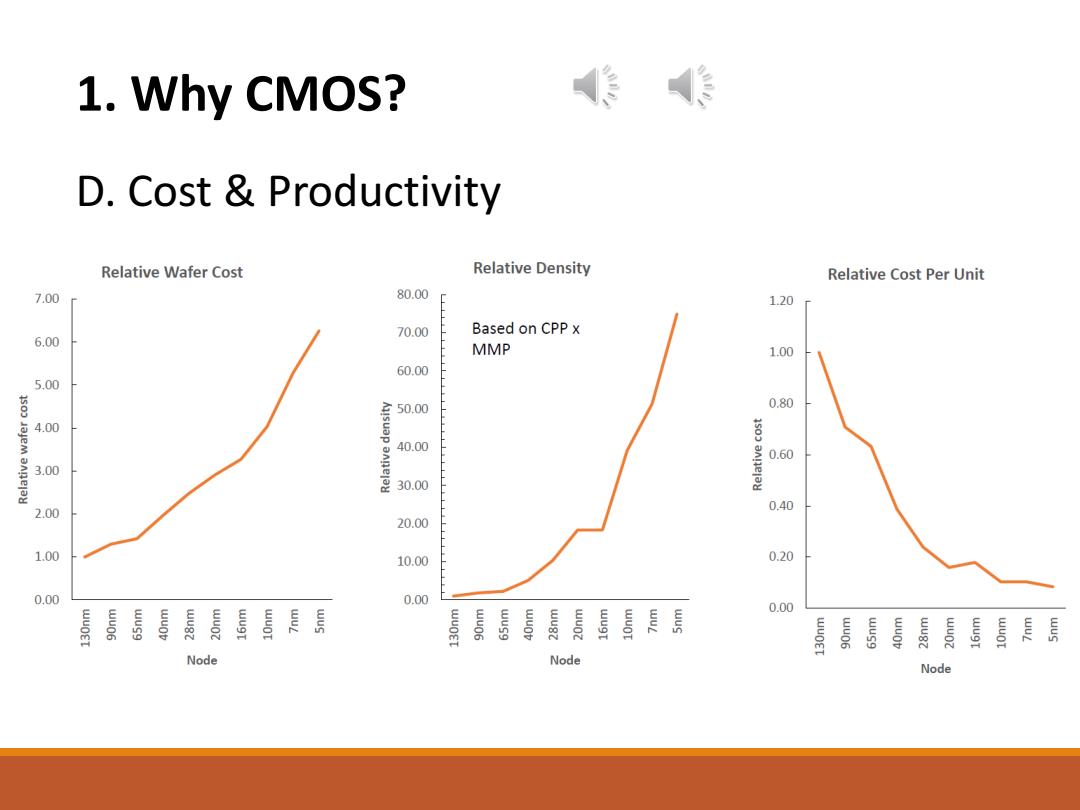
1.Why CMOS? 作 D.Cost Productivity Relative Wafer Cost Relative Density Relative Cost Per Unit 7.00 80.00 1.20 70.00 Based on CPP x 6.00 MMP 1.00 60.00 5.00 0.80 4.00 40.00 0.60 3.00 30.00 2.00 0.40 20.00 1.00 10.00 020 0.00 0.00 0.00 Node Node Node
1. Why CMOS? D. Cost & Productivity
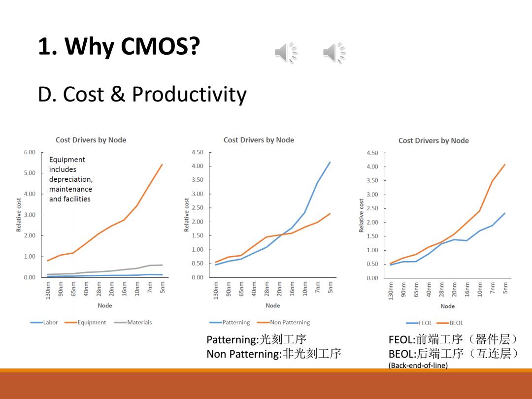
1.Why CMOS? D.Cost Productivity Cost Drivers by Node Cost Drivers by Node Cost Drivers by Node 6.00 4.50 4.50 Equipment includes 4.00 4.00 5.00 depreciation, 3.50 3.50 maintenance 4.00 3.00 3.00 and facilities 2.50 3.00 2.00 annelay 2.00 2.00 1.50 1.50 1.00 1.00 1.00 0.50 0.50 0.00 0.00 0.00 Node Node Node Equipment Materials -Patterning -Non Patterning Patterning:光刻工序 FEOL:前端工序(器件层) Non Patterning:非光刻工序 BEOL:后端工序(互连层) (Back-end-of-line)
1. Why CMOS? D. Cost & Productivity Patterning:光刻工序 Non Patterning:非光刻工序 FEOL:前端工序(器件层) BEOL:后端工序(互连层) (Back-end-of-line)

2.CMOS Process 传 Poly G B S D Oxide p W p+ n+ nt Leff p-substrate -drawn
2. CMOS Process
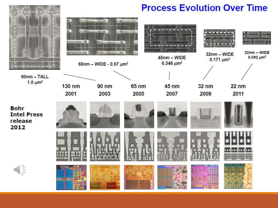
Process Evolution Over Time 32nm-WIDE 22nm-WIDE 45nm-WIDE 0.171m2 0.0924m2 65nm-WIDE-0.57 um2 0.346μm2 90nm-TALL 1.0μm2 130nm 90 nm 65 nm 45 nm 32 nm 22 nm 2001 2003 2005 2007 2009 2011 Bohr Intel Press release 2012
2. CMOS Process
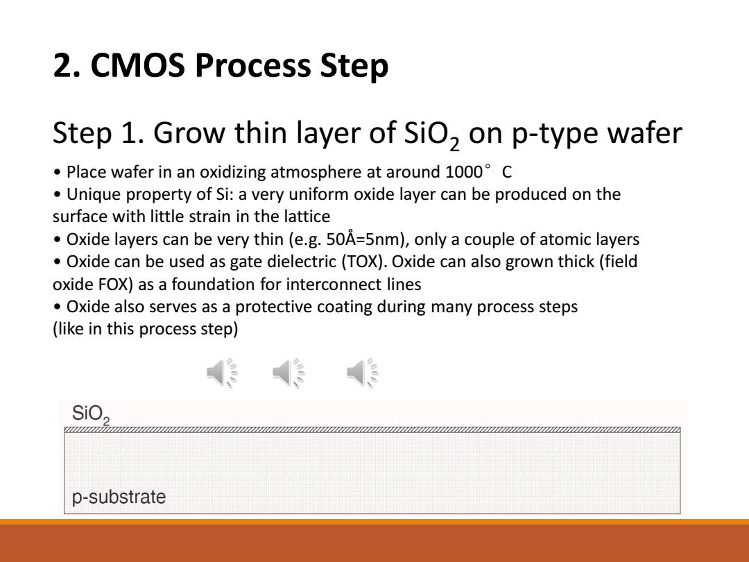
2.CMOS Process Step Step 1.Grow thin layer of SiO,on p-type wafer Place wafer in an oxidizing atmosphere at around 1000C Unique property of Si:a very uniform oxide layer can be produced on the surface with little strain in the lattice Oxide layers can be very thin (e.g.50A=5nm),only a couple of atomic layers Oxide can be used as gate dielectric(TOX).Oxide can also grown thick(field oxide FOX)as a foundation for interconnect lines Oxide also serves as a protective coating during many process steps (like in this process step) SiO, p-substrate
2. CMOS Process Step Step 1. Grow thin layer of SiO2 on p-type wafer • Place wafer in an oxidizing atmosphere at around 1000°C • Unique property of Si: a very uniform oxide layer can be produced on the surface with little strain in the lattice • Oxide layers can be very thin (e.g. 50Å=5nm), only a couple of atomic layers • Oxide can be used as gate dielectric (TOX). Oxide can also grown thick (field oxide FOX) as a foundation for interconnect lines • Oxide also serves as a protective coating during many process steps (like in this process step)