第八讲 Passive devices 游飞博导/副教授,电子科技大学 feiyou@uestc.edu.cn
第八讲 Passive Devices 游飞 博导/副教授,电子科技大学 feiyou@uestc.edu.cn
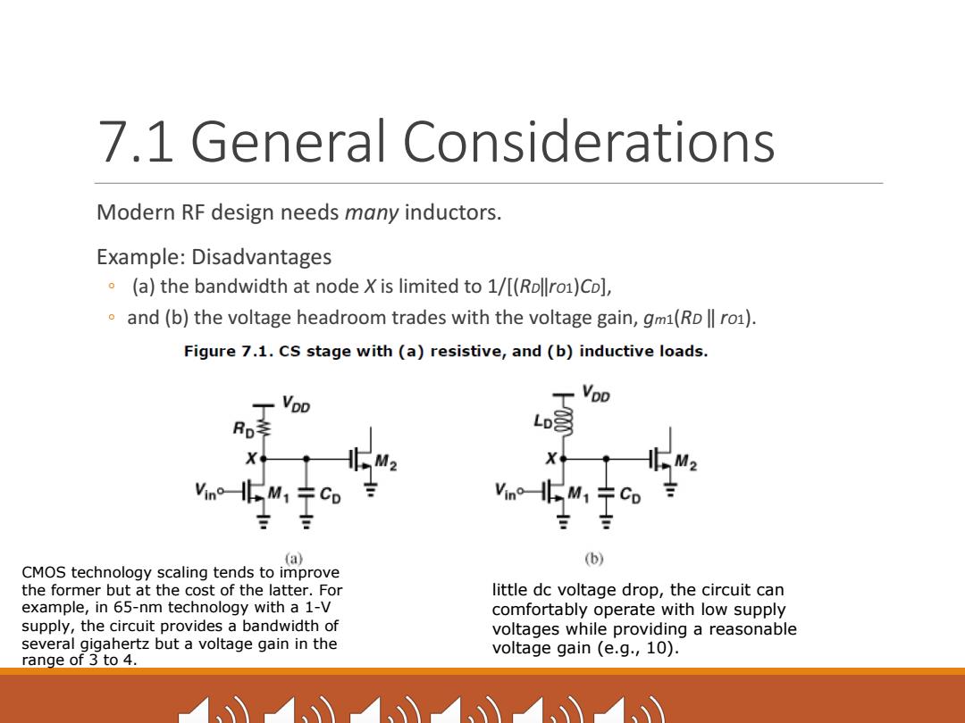
7.1 General Considerations Modern RF design needs many inductors. Example:Disadvantages (a)the bandwidth at node X is limited to 1/[(RDllro1)Co], and(b)the voltage headroom trades with the voltage gain,gm1(RDll ro1). Figure 7.1.CS stage with (a)resistive,and (b)inductive loads. (a) (b) CMOS technology scaling tends to improve the former but at the cost of the latter.For little dc voltage drop,the circuit can example,in 65-nm technology with a 1-V comfortably operate with low supply supply,the circuit provides a bandwidth of voltages while providing a reasonable several gigahertz but a voltage gain in the voltage gain (e.g.,10). range of 3 to 4
7.1 General Considerations Modern RF design needs many inductors. Example: Disadvantages ◦ (a) the bandwidth at node X is limited to 1/[(RD‖rO1)CD], ◦ and (b) the voltage headroom trades with the voltage gain, gm1(RD ‖ rO1). CMOS technology scaling tends to improve the former but at the cost of the latter. For example, in 65-nm technology with a 1-V supply, the circuit provides a bandwidth of several gigahertz but a voltage gain in the range of 3 to 4. little dc voltage drop, the circuit can comfortably operate with low supply voltages while providing a reasonable voltage gain (e.g., 10)
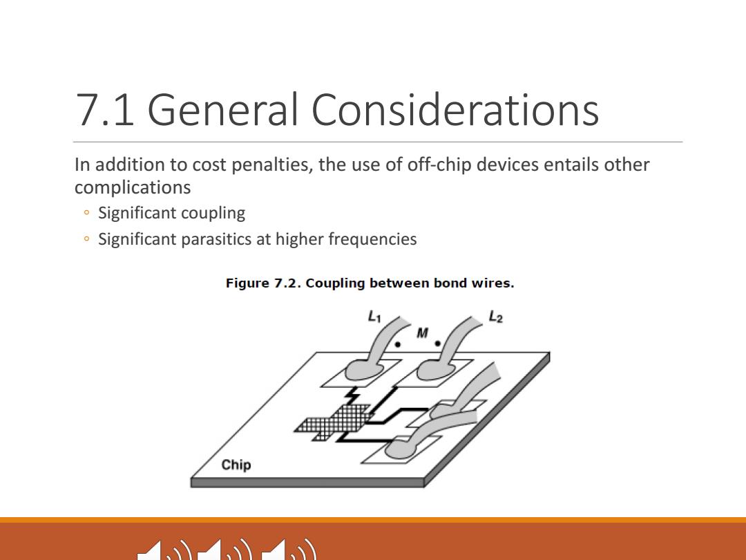
7.1 General Considerations In addition to cost penalties,the use of off-chip devices entails other complications Significant coupling Significant parasitics at higher frequencies Figure 7.2.Coupling between bond wires. Chip
7.1 General Considerations In addition to cost penalties, the use of off-chip devices entails other complications ◦ Significant coupling ◦ Significant parasitics at higher frequencies

7.1 General Considerations Identify two undesirable coupling mechanisms if the LO inductor is placed off-chip. Figure 7.3.Hypothetical transceiver using an off-chip inductor. Bond Wire LNA Off-Chip Inductor -1000
7.1 General Considerations Identify two undesirable coupling mechanisms if the LO inductor is placed off-chip
7.1 General Considerations Modeling Issues inductors and some other structures are much more difficult to model. In fact,the required modeling effort proves a high barrier to entry into RF design: one cannot add an inductor to a circuit without an accurate model, and the model heavily depends on the geometry,the layout,and the technology's metal layers (which is the thickest)
7.1 General Considerations Modeling Issues ◦ inductors and some other structures are much more difficult to model. ◦ In fact, the required modeling effort proves a high barrier to entry into RF design: ◦ one cannot add an inductor to a circuit without an accurate model, ◦ and the model heavily depends on the geometry, the layout, and the technology’s metal layers (which is the thickest)