Experiment 5 Properties of Silicon Photocell and Solar Cell One of the very important properties of semiconductor is its ability to convert photo energy to electronic energy without external power.Photocell and Solar cell are two typical applications utilizing this ability.Photocell can be made by Selenium,Germanium,Silicon,Gallium Arsenide and so on.Among them,the Silicon photocell (abbreviated as SPC)is the most widely used. Silicon photocell is very stable,high efficient,wide spectrum response,high working temperature and resistance to radiation.Interestingly,the sensitivity of the silicon photocell is very similar with human being's eyes. Solar cell is known as photovoltaic cell.Solar cells can be packaged into solar cell components that can be integrated according to the power requirement.Combined with energy storage devices, controlling device,DC-AC converter and so on,we can build solar power plants.Solar cell is renewable and clear energy system.The world's first practical semiconductor solar cells were developed by Bell Laboratories in the U.S.in 1954.After 50 years,the research and applications of solar cell had made tremendous progress.As the costs of solar cells decrease continuously, solar power plants will gradually partly replace conventional power plants.Very recently,solar power plants have entered the state grid in China. This experiment is the research of basic properties of the SPC and the solar cell. 【Objectives】. 1.Understand the principle of the SPC. 2.Study the basic properties and parameters of SPC. 3.Understand the principle of solar cell. 4.Study the Volt-Ampere characteristics of solar cell 【Principle】 1.Photovoltaic effect When the light with photon energy greater than the band gap(Eg)of the semiconductor irradiates on a PN junction,photons will be absorbed in the p-type region,the n-type region as well as the junction region,which generates lots of free carriers including electrons and holes. Minority carriers in the n-type or p-type region near the junction will diffuse due to the concentration gradient.If the distance between minority carriers and the PN-junction region is less than its diffusion length,there is always a chance for the carriers to diffuse to the PN interface.Near the PN interface (junction region),there is a space charge layer known as the -1-
- 1 - Experiment 5 Properties of Silicon Photocell and Solar Cell One of the very important properties of semiconductor is its ability to convert photo energy to electronic energy without external power. Photocell and Solar cell are two typical applications utilizing this ability. Photocell can be made by Selenium, Germanium, Silicon, Gallium Arsenide and so on. Among them, the Silicon photocell (abbreviated as SPC) is the most widely used. Silicon photocell is very stable, high efficient, wide spectrum response, high working temperature and resistance to radiation. Interestingly, the sensitivity of the silicon photocell is very similar with human being's eyes. Solar cell is known as photovoltaic cell. Solar cells can be packaged into solar cell components that can be integrated according to the power requirement. Combined with energy storage devices, controlling device, DC-AC converter and so on, we can build solar power plants. Solar cell is renewable and clear energy system. The world's first practical semiconductor solar cells were developed by Bell Laboratories in the U.S. in 1954. After 50 years, the research and applications of solar cell had made tremendous progress. As the costs of solar cells decrease continuously, solar power plants will gradually partly replace conventional power plants. Very recently, solar power plants have entered the state grid in China. This experiment is the research of basic properties of the SPC and the solar cell. 【Objectives】 1. Understand the principle of the SPC. 2. Study the basic properties and parameters of SPC. 3. Understand the principle of solar cell. 4. Study the Volt-Ampere characteristics of solar cell. 【Principle】 1. Photovoltaic effect When the light with photon energy greater than the band gap (Eg) of the semiconductor irradiates on a PN junction, photons will be absorbed in the p-type region, the n-type region as well as the junction region, which generates lots of free carriers including electrons and holes. Minority carriers in the n-type or p-type region near the junction will diffuse due to the concentration gradient. If the distance between minority carriers and the PN-junction region is less than its diffusion length, there is always a chance for the carriers to diffuse to the PN interface. Near the PN interface (junction region), there is a space charge layer known as the

depletion region or depletion layer.There is an electric field in the depletion region pointing toward p-type region from the n-type region.This electric field is called built-in electric field. Holes in the n-type region near the PN-junction spread to the PN interface are pulled to the p-type region by the built-in electric field.Due to the same principle,electrons in the p-type region near the junction are pulled to the n-type region.The electrons and holes in the junction region move towards the n-and p-type region respectively.If the external circuit is open, photo-induced electrons and holes can accumulate near the PN junction,which builds up a stable potential difference,called optical electromotive force.This phenomenon is known as the photovoltaic effect(abbreviated as PV). 2.Photocell The SPC is a silicon-based device that converts the photo energy to the electricity utilizing photovoltaic effect.The key part of SPC is a PN junction with very large area.Because the PN junction area in SPC is much larger than that in normal diode,the photoelectric current of is very large.For example,exposed to 1000 luminous light,the SPC(made in china,model 2DU10) used in our experiment can created the 300mV of open-circuit voltage or 50mA short-circuit current 1)Structure of SPC 灵敏面积 The typical structure of a SPC is shown P扩散 in the Fig.1. n-型硅体积 耗尽区 2)The illumination characteristics of SPC n扩散 (1)short-circuit current and illumination 金属接触 When the SPC is under illumination,there is a photo-induced current /ph from the N area Figure 1 Typical P-N structure of silicon photocell to P area.As a diode,there is a forward diode current /p from P area to the N area,which is opposite to the Iph.As a result,the total current should be (1) V is the junction voltage.lo means inverse saturation current without illumination.I Ph is proportional to the illumination intensity.The factor of proportionality is related to the load and -2-
- 2 - depletion region or depletion layer. There is an electric field in the depletion region pointing toward p-type region from the n-type region. This electric field is called built-in electric field. Holes in the n-type region near the PN-junction spread to the PN interface are pulled to the p-type region by the built-in electric field. Due to the same principle, electrons in the p-type region near the junction are pulled to the n-type region. The electrons and holes in the junction region move towards the n-and p-type region respectively. If the external circuit is open, photo-induced electrons and holes can accumulate near the PN junction, which builds up a stable potential difference, called optical electromotive force. This phenomenon is known as the photovoltaic effect (abbreviated as PV). 2. Photocell The SPC is a silicon-based device that converts the photo energy to the electricity utilizing photovoltaic effect. The key part of SPC is a PN junction with very large area. Because the PN junction area in SPC is much larger than that in normal diode, the photoelectric current of is very large. For example, exposed to 1000 luminous light, the SPC (made in china, model 2DU10) used in our experiment can created the 300mV of open-circuit voltage or 50mA short-circuit current 1) Structure of SPC The typical structure of a SPC is shown in the Fig. 1. 2) The illumination characteristics of SPC (1) short- circuit current and illumination When the SPC is under illumination, there is a photo-induced current IPh from the N area to P area. As a diode, there is a forward diode current ID from P area to the N area, which is opposite to the IPh. As a result, the total current should be ⎥ ⎥ ⎦ ⎤ ⎢ ⎢ ⎣ ⎡ −⎟ ⎟ ⎠ ⎞ ⎜ ⎜ ⎝ ⎛ = − = − 1 n 0 exp k T qV I I I I I B Ph D Ph (1) V is the junction voltage. I0 means inverse saturation current without illumination. I Ph is proportional to the illumination intensity. The factor of proportionality is related to the load and Figure 1 Typical P-N structure of silicon photocell
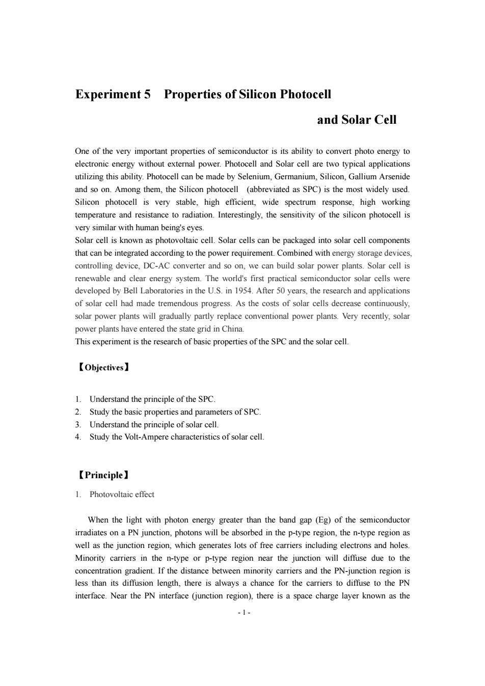
the structure and material of SPC.n is the ideality factor,which is between I to 2.q is the electron's charge.kB is the Boltzmann constant.T is the temperature of the junction.Under certain illumination,if the SPC is short,then V=0.We can get the short circuit current. Isc =Iph (2) Figure 2 presents SPC's short circuit current as a function of illumination. (2)open circuit voltage and illumination of SPC If the SPC is open circuit,then I=0.From Equation 1 and 2,we get the open circuit voltage nk T (3) q Figure 2 presents SPC's open circuit voltage as a function of illumination. Uoe/Vt 开路电压 牛Isc/uA 0.5 20 0.4 16 0.3 短路电流 白 0.2 8 0.1 4 0 200040006000800010000 E/Lux (a)Inverse-bias condition (b)Non-biased condition Figure 2 Properties of silicon photocell as a function of Figure 3 Two basic work conditions for silicon Illumination photocell 3)The I-V character of SPC Different from the normal diode,the SPC usually work under the inverse-biased condition(Fig 3a)or non-biased condition(Fig 3b).When the SPC is connected with a load RL,its I-V curve is shown in Fig.4.Even under the inverse bias or non-bias condition,there is a backward current, which is the main difference between SPC and the normal diode.Without illumination,there is a very small backward leading current that is called dark current. (1)Inverse-bias(Third quadrant in the Fig.4) Under the inverse bias condition,for a wide range of applied voltage and load resistance,the photoelectric current linearly depends on the power of incident light.Since the photoelectric current is nearly independent to the bias voltage and load resistance within a very large dynamic -3-
- 3 - the structure and material of SPC. n is the ideality factor, which is between 1 to 2. q is the electron’s charge. kB is the Boltzmann constant. T is the temperature of the junction. Under certain illumination, if the SPC is short, then V=0. We can get the short circuit current. SC Ph I = I (2) Figure 2 presents SPC’s short circuit current as a function of illumination. (2) open circuit voltage and illumination of SPC If the SPC is open circuit, then I=0. From Equation 1 and 2, we get the open circuit voltage ⎟ ⎟ ⎠ ⎞ ⎜ ⎜ ⎝ ⎛ = ln +1 0 I I q nk T V B SC OC (3) Figure 2 presents SPC’s open circuit voltage as a function of illumination. 3) The I-V character of SPC Different from the normal diode, the SPC usually work under the inverse-biased condition (Fig 3a) or non-biased condition (Fig 3b). When the SPC is connected with a load RL, its I-V curve is shown in Fig.4. Even under the inverse bias or non-bias condition, there is a backward current, which is the main difference between SPC and the normal diode. Without illumination, there is a very small backward leading current that is called dark current. (1) Inverse-bias (Third quadrant in the Fig. 4) Under the inverse bias condition, for a wide range of applied voltage and load resistance, the photoelectric current linearly depends on the power of incident light. Since the photoelectric current is nearly independent to the bias voltage and load resistance within a very large dynamic Figure 2 Properties of silicon photocell as a function of Illumination (a)Inverse-bias condition(b)Non-biased condition Figure 3 Two basic work conditions for silicon photocell

range,the SPC can be treated as a constant current source when the power of the incident light is certain. (2)non-bias (Fourth quadrant in the Fig.4) Under the non-bias state condition,the photoelectric current is proportional to the power of incident light only if the RL is small.As the RL increase,the relation between the photoelectric current and the power of incident light becomes nonlinear.The relation between the short-circuit current and the power of incident light without bias voltage is called the photoelectric character UN3.02.52.0-1.51.0-0.50 10020030p400 U/mV -5 R大 -10 -15 E2 -201 Es -25 R小 Ea 反向偏压工作区 1/uA 无偏压工作因 Figure 4 I-V curves of silicon photocells of SPC.The slope in the IL-P coordinator is defined as the SPC's responsiveness.R is a very important parameter to characterize the photoelectric conversion efficiency macroscopically. R=AIL (4) AP (A/w) Under non-bias condition,the SPC is not a constant current source when the load resistance varies a lot.It is just like a battery. Seen from the Fig.4,for each illumination,the intercept of load curve on the current axis is the short-circuit current Iph.The intercept on the voltage axis is the open voltage Voc 4)*Spectral response of SPC Figure 5 is the spectral characteristic curve of SPC.The vertical axis is the relative sensitivity Kr and the abscissa axis is the wavelength A From the Fig.5 we can see that the effective range of SPC is about from 450nm to 1100nm Sensitivity of SPC is defined as P(2) K=0T0)△M (5) -4-
- 4 - range, the SPC can be treated as a constant current source when the power of the incident light is certain. (2) non-bias (Fourth quadrant in the Fig.4) Under the non-bias state condition, the photoelectric current is proportional to the power of incident light only if the RL is small. As the RL increase, the relation between the photoelectric current and the power of incident light becomes nonlinear. The relation between the short-circuit current and the power of incident light without bias voltage is called the photoelectric character of SPC. The slope in the IL-P coordinator is defined as the SPC's responsiveness. R is a very important parameter to characterize the photoelectric conversion efficiency macroscopically. ( ) A / w Δ Δ μ μ P I R L = (4) Under non-bias condition, the SPC is not a constant current source when the load resistance varies a lot. It is just like a battery. Seen from the Fig.4, for each illumination, the intercept of load curve on the current axis is the short-circuit current IPh. The intercept on the voltage axis is the open voltage VOC 4) * Spectral response of SPC Figure 5 is the spectral characteristic curve of SPC. The vertical axis is the relative sensitivity Kr and the abscissa axis is the wavelength λ. From the Fig. 5 we can see that the effective range of SPC is about from 450nm to 1100nm Sensitivity of SPC is defined as ( ) ( ) η() () λ λ λ λ λ Δ = T P K (5) -0.5 0 100 200 300 400 -5 -10 -15 -20 -25 RL 大 反向偏压工作区 无偏压工作区 E3 E2 E1 U / V -3.0 -2.5 -2.0 -1.5 -1.0 U / mV E4 I / A RL 小 Figure 4 I-V curves of silicon photocells
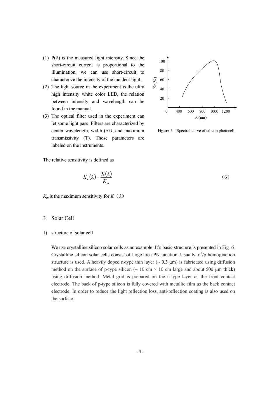
(1)P()is the measured light intensity.Since the 100 short-circuit current is proportional to the illumination,we can use short-circuit to 80 characterize the intensity of the incident light. 60 (2)The light source in the experiment is the ultra 立 40 high intensity white color LED,the relation 20 between intensity and wavelength can be found in the manual. 0 400600800 10001200 (3)The optical filter used in the experiment can 元(nm) let some light pass.Filters are characterized by center wavelength,width (AN,and maximum Figure 5 Spectral curve of silicon photocell transmissivity (T).Those parameters are labeled on the instruments. The relative sensitivity is defined as K()=K(a) (6) Kn K is the maximum sensitivity for K ( 3. Solar Cell 1)structure of solar cell We use crystalline silicon solar cells as an example.It's basic structure is presented in Fig.6. Crystalline silicon solar cells consist of large-area PN junction.Usually,n/p homojunction structure is used.A heavily doped n-type thin layer(~0.3 um)is fabricated using diffusion method on the surface of p-type silicon(~10 cm x 10 cm large and about 500 um thick) using diffusion method.Metal grid is prepared on the n-type layer as the front contact electrode.The back of p-type silicon is fully covered with metallic film as the back contact electrode.In order to reduce the light reflection loss,anti-reflection coating is also used on the surface. -5-
- 5 - (1) P(λ) is the measured light intensity. Since the short-circuit current is proportional to the illumination, we can use short-circuit to characterize the intensity of the incident light. (2) The light source in the experiment is the ultra high intensity white color LED, the relation between intensity and wavelength can be found in the manual. (3) The optical filter used in the experiment can let some light pass. Filters are characterized by center wavelength, width (∆λ), and maximum transmissivity (T). Those parameters are labeled on the instruments. The relative sensitivity is defined as ( ) ( ) m r K K K λ λ = (6) Km is the maximum sensitivity for K(λ) 3. Solar Cell 1) structure of solar cell We use crystalline silicon solar cells as an example. It’s basic structure is presented in Fig. 6. Crystalline silicon solar cells consist of large-area PN junction. Usually, n+ /p homojunction structure is used. A heavily doped n-type thin layer (~ 0.3 µm) is fabricated using diffusion method on the surface of p-type silicon (~ 10 cm × 10 cm large and about 500 µm thick) using diffusion method. Metal grid is prepared on the n-type layer as the front contact electrode. The back of p-type silicon is fully covered with metallic film as the back contact electrode. In order to reduce the light reflection loss, anti-reflection coating is also used on the surface. 20 40 60 80 100 0 400 600 800 1000 1200 Kr %( ) nm Figure 5 Spectral curve of silicon photocell