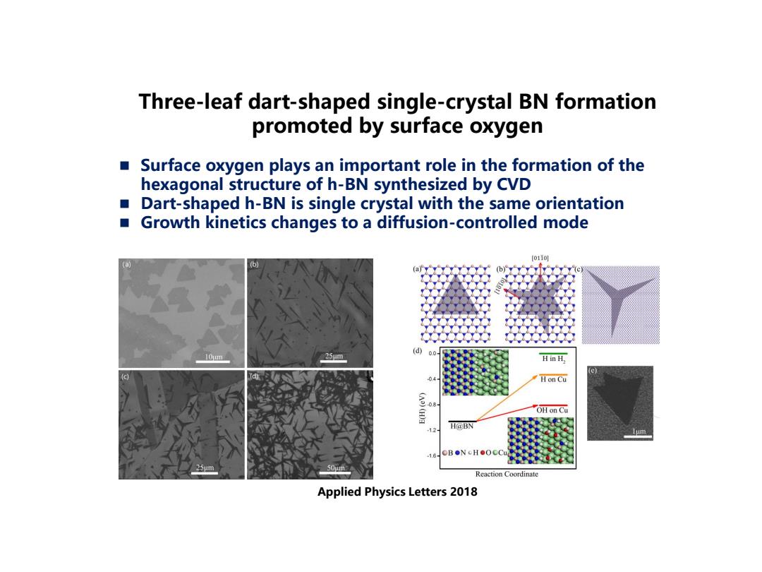
Three-leaf dart-shaped single-crystal BN formation promoted by surface oxygen ■ Surface oxygen plays an important role in the formation of the hexagonal structure of h-BN synthesized by CVD Dart-shaped h-BN is single crystal with the same orientation Growth kinetics changes to a diffusion-controlled mode 110 (d)00 10m 25m H in H, 04 Hon Cu OH on Cu -12 H@BN -1.6 50m Reaction Coordinate Applied Physics Letters 2018
Three-leaf dart-shaped single-crystal BN formation 2.5 promoted by surface oxygen ◼ Surface oxygen plays an important role in the formation of the hexagonal structure of h-BN synthesized by CVD ◼ Dart-shaped h-BN is single crystal with the same orientation ◼ Growth kinetics changes to a diffusion-controlled mode Applied Physics Letters 2018
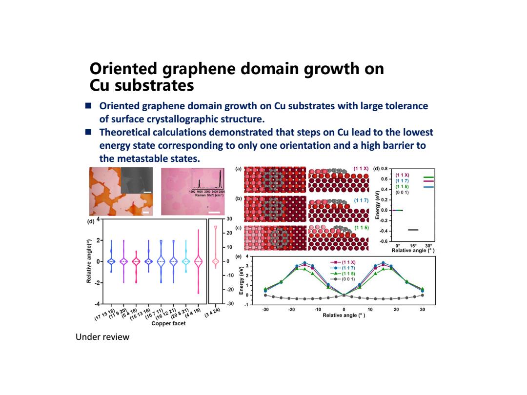
Oriented graphene domain growth on Cu substrates ■ Oriented graphene domain growth on Cu substrates with large tolerance of surface crystallographic structure. Theoretical calculations demonstrated that steps on Cu lead to the lowest energy state corresponding to only one orientation and a high barrier to the metastable states. (a) (11)d0.8 (11) 0.6 117) 115) 010020002002 0.4 (001) (b (117刀 02 (d) 30 0.2 (c) (115) 0.4 粉 0.6 0°1530 Relative angle() (e) 11X 10 (A) -117刀 -(115) -001)】 20 -30 -30 -10 10 20 Relative angle(e)】 Copper facet Under review
Oriented graphene domain growth on Cu substrates ◼ Oriented graphene domain growth on Cu substrates with large tolerance of surface crystallographic structure. ◼ Theoretical calculations demonstrated that steps on Cu lead to the lowest energy state corresponding to only one orientation and a high barrier to the metastable states. Under review 2.6
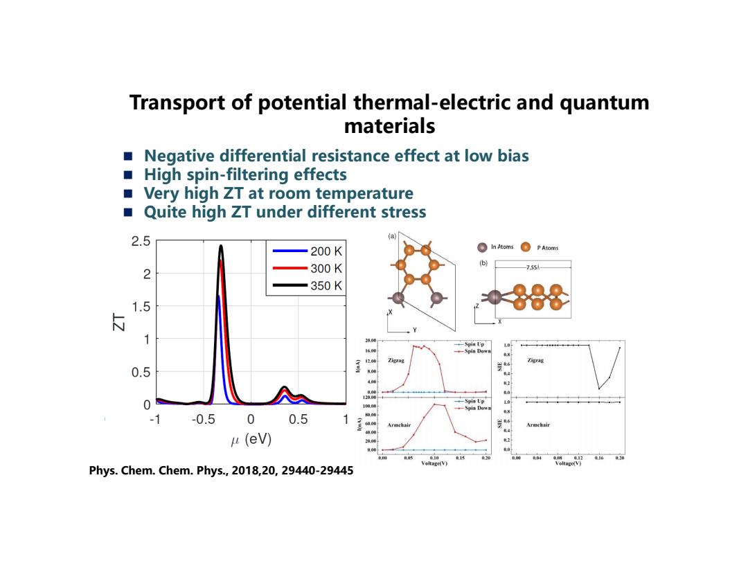
Transport of potential thermal-electric and quantum materials ■ Negative differential resistance effect at low bias High spin-filtering effects ■ Very high ZT at room temperature ■ Quite high ZT under different stress 2.5 (a) 200K In Atoms PAtoms 300K (b) 755到 2 350K 1.5 888 1 20 Spin Up 1.0- 6用 +一5DnD和特 0.5 4 2 0 Spie Up 19000 10 -1 -0.5 0 0.5 1 o. Armchair μ(eV) 0.10 1 Voltage(V门 Voltage(V) Phys.Chem.Chem.Phys.,2018,20,29440-29445
Transport of potential thermal-electric and quantum 2.7 materials Phys. Chem. Chem. Phys., 2018,20, 29440-29445 ◼ Negative differential resistance effect at low bias ◼ High spin-filtering effects ◼ Very high ZT at room temperature ◼ Quite high ZT under different stress
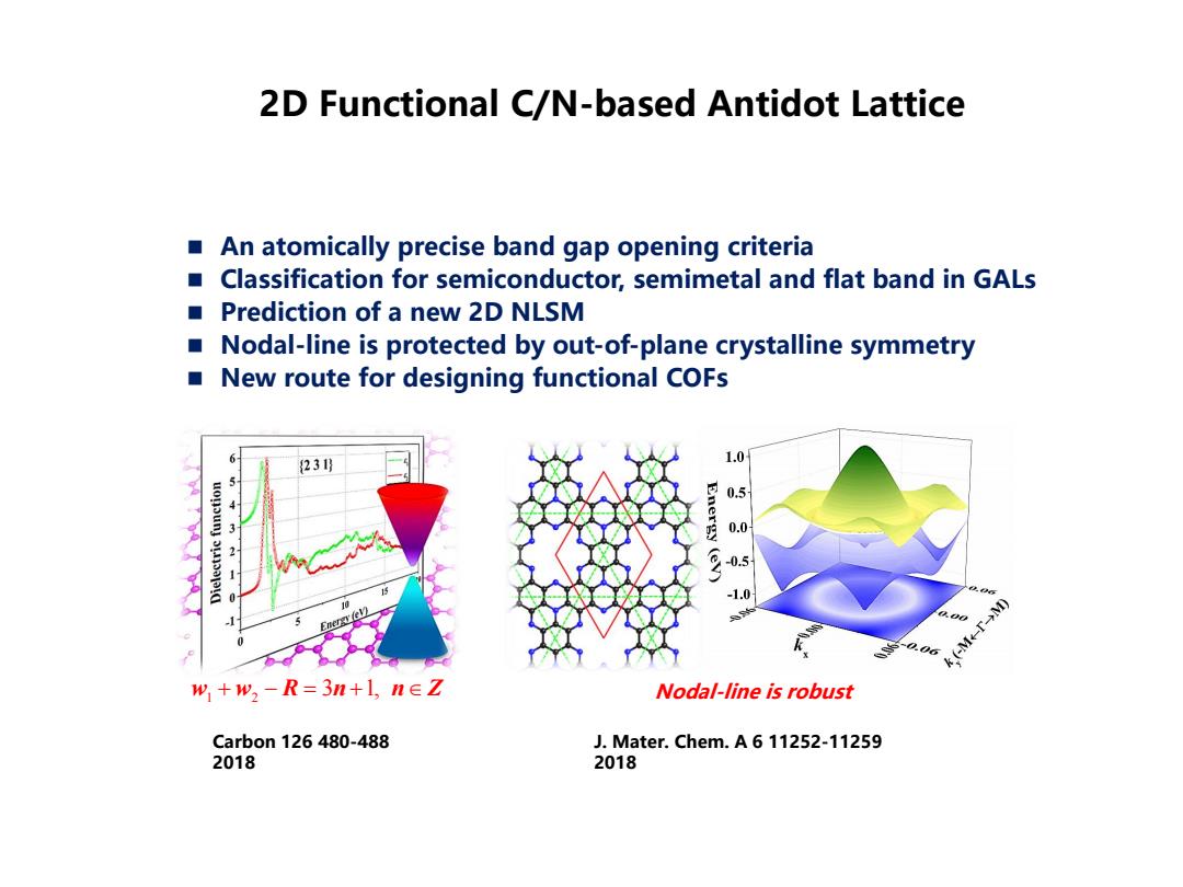
2D Functional C/N-based Antidot Lattice An atomically precise band gap opening criteria Classification for semiconductor,semimetal and flat band in GALs Prediction of a new 2D NLSM ■ Nodal-line is protected by out-of-plane crystalline symmetry ■ New route for designing functional COFs 230 L.0 54 0.5 3 0.0 2 Energy (ev) 0.5 -1.0 10 -2.06 (-Me w,+w2-R=3n+l,n∈Z Nodal-line is robust Carbon126480-488 J.Mater.Chem.A 6 11252-11259 2018 2018
2D Functional C/N-based Antidot Lattice 2.8 J. Mater. Chem. A 6 11252-11259 2018 Carbon 126 480-488 2018 w w R n n Z 1 2 + − = + 3 1, Nodal-line is robust ◼ An atomically precise band gap opening criteria ◼ Classification for semiconductor, semimetal and flat band in GALs ◼ Prediction of a new 2D NLSM ◼ Nodal-line is protected by out-of-plane crystalline symmetry ◼ New route for designing functional COFs

Band Regulation of Graphene Heterojunction ■ Energy band regulation by adjusting the width of graphene nanoribbons Energy band regulation by Controlling defect's shape and distance Both Type-l and Type ll band-order matching are realized through the adjustment of intrinsic graphene 3 -30524 34318 354916 358146 3.6514 3.66134 38858 -398339 -4 4.16358 42082 433227 4479羽 4.44242 457725 456882 -5 509425
Band Regulation of Graphene Heterojunction ◼ Energy band regulation by adjusting the width of graphene nanoribbons ◼ Energy band regulation by Controlling defect’s shape and distance ◼ Both Type-I and Type II band-order matching are realized through the adjustment of intrinsic graphene 2.9