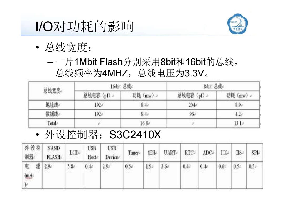
/O对功耗的影响 ·总线宽度: 一片1 Mbit Flash分别采用8bit和16bit的总线, 总线频率为4MHZ,总线电压为3.3V。 16-b址t总线 8-bt总线 总线宽度 总线电容(pD。 功耗(nw), 总线电容(pfD。 功耗(w)。 地址线 192e 84 204 89 数据绒 192 84 96 42 Total 168 131 外设控制器:S3C2410X 外设控 NAND USB USB LCD. Tier SDI UART RTC ADC. IIC S SPI 制器 FLASH. Host. Device 电流20 5.8 04 29 05 19 3.6 04+ 04 0.6 0.5. 0.5 (mA
I/O对功耗的影响 • 总线宽度: – 一片1Mbit Flash分别采用8bit和16bit的总线, 总线频率为4MHZ,总线电压为3.3V。 • llxx@ustc.edu.cn 16/62 • 外设控制器:S3C2410X
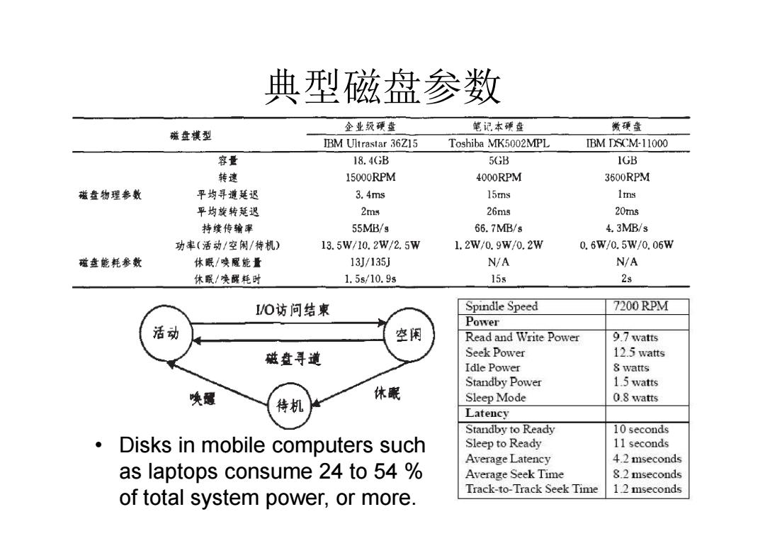
典型磁盘参数 滋盘模型 企业级硬盘 笔记本硬盘 微硬盘 IBM Ultrastar 36Z15 Toshiba MK5002MPL IBM DSCM-11000 容量 18.4(B 5GB 1GB 转速 15000RPM 4000RPM 3600RPM 磁盘物理参数 平均寻道延迟 3.4ms 15ms 1ms 平均旋转延迟 2ms 26ms 20ms 持续传输率 55MB/g 66.7MB/s 4.3MB/s 功率(活动/空闲/特机) 13.5W/10.2W/2.5W 1.2W/0.9w/0.2W 0.6W/0.5W/0.06W 磁盘能耗参数 休眠/唤醒能量 13J/135J N/A N/A 休眠/唤醒花时 1.5s/10.9s 15s 2s I/O访问结柬 Spindle Speed 7200 RPM Power 活动 空闲 Read and Write Power 9.7 watts 磁查寻道 Seek Power 12.5 watts Idle Power 8 watts Standby Power 1.5 watts 唤露 休眼 待机 Sleep Mode 0.8 watts Latency Standby to Ready 10 seconds Disks in mobile computers such Sleep to Ready 11 seconds Average Latency 4.2 mseconds as laptops consume 24 to 54 Average Seek Time 8.2 mseconds Track-to-Track Seek Time 1.2 mseconds of total system power,or more
典型磁盘参数 • Disks in mobile computers such as laptops consume 24 to 54 % of total system power, or more
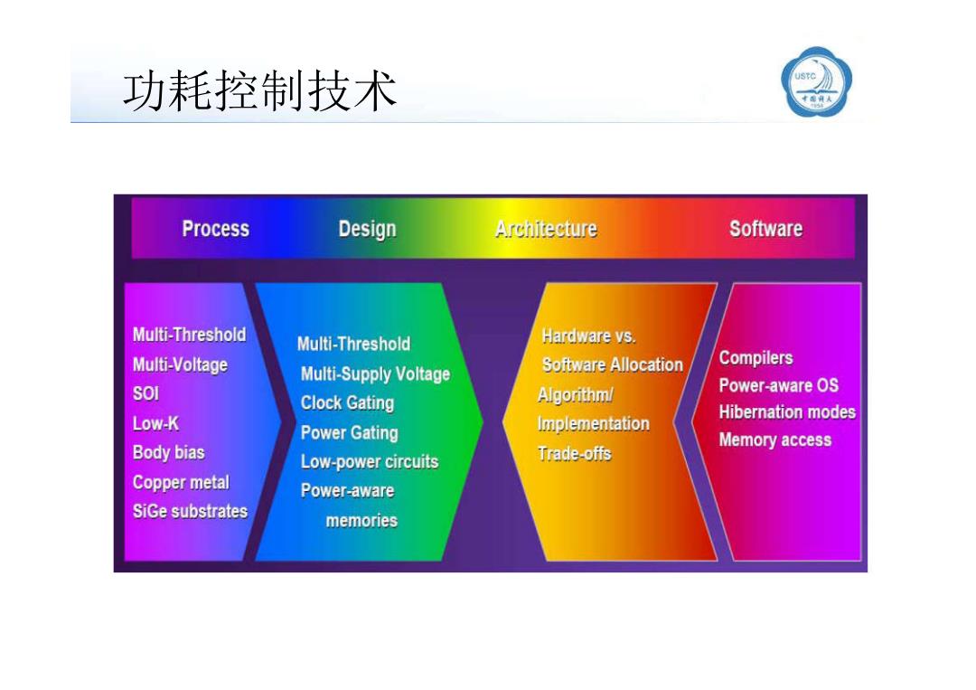
功耗控制技术 Process Design Architecture Software Multi-Threshold Multi-Threshold Hardware vs. Multi-Voltage Multi-Supply Voltage Software Allocation Compilers SOI Clock Gating Algorithm/ Power-aware OS Low-K Hibernation modes Power Gating Implementation Body bias Memory access Low-power circuits Trade-offs Copper metal Power-aware SiGe substrates memories
功耗控制技术
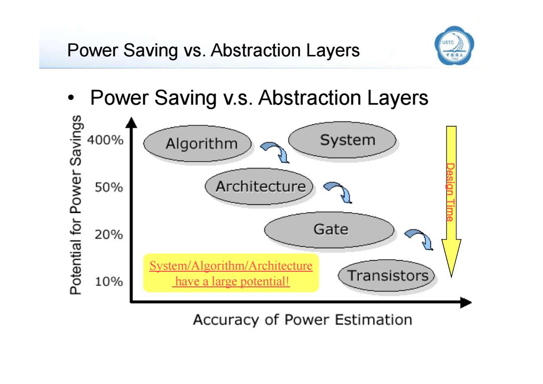
USTC Power Saving vs.Abstraction Layers Power Saving v.s.Abstraction Layers 400% Algorithm System 50% Architecture Desian Time 20% Gate System/Algorithm/Architecture 10% have a large potential! Transistors Accuracy of Power Estimation
Power Saving vs. Abstraction Layers • Power Saving v.s. Abstraction Layers Design Time System/Algorithm/Architecture have a large potential!
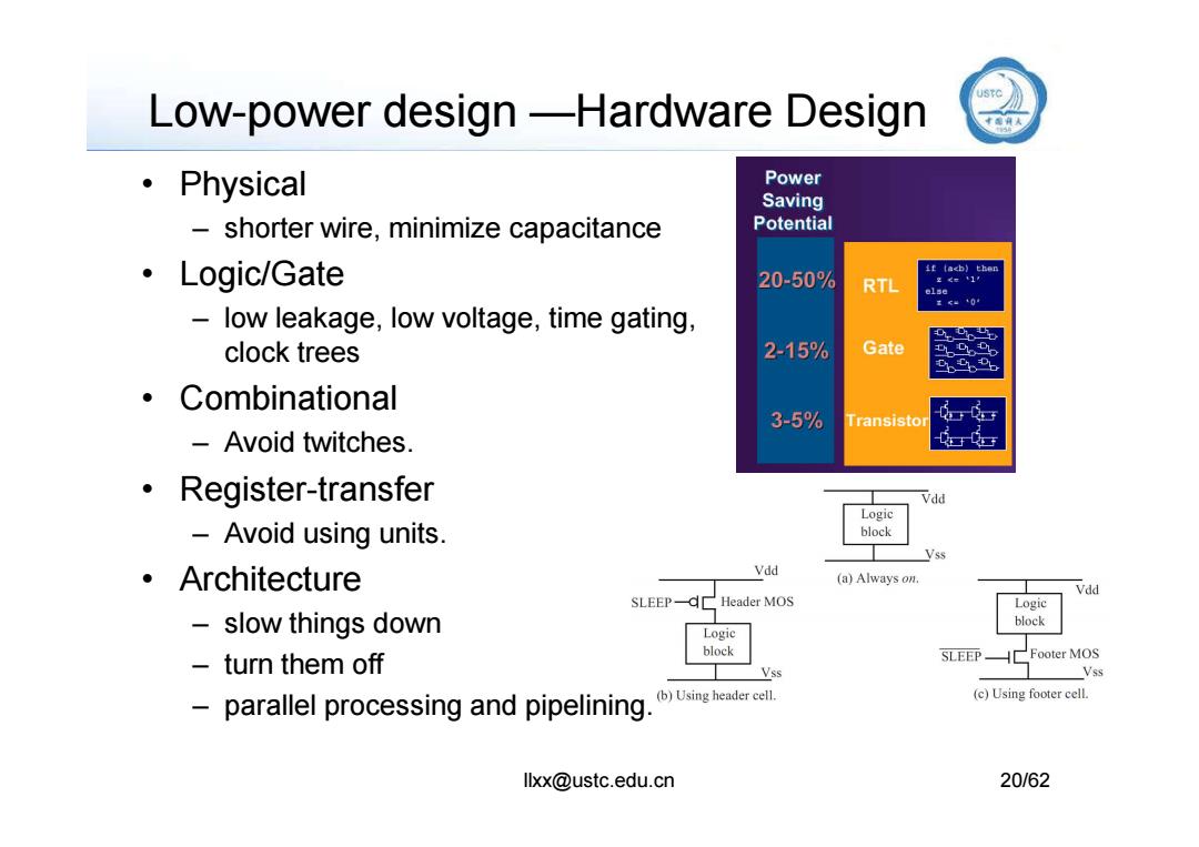
Low-power design-Hardware Design ·Physical Power Saving -shorter wire,minimize capacitance Potential ·Logic/Gate it tacb)then 20-50% RTL else low leakage,low voltage,time gating, clock trees 2-15% Gate 。Combinational 3-5% Transistor -Avoid twitches. ·Register-.transfer Logic Avoid using units. block Vss ·Architecture Vdd (a)Always on. Vdd SLEEP-Header MOS Logic slow things down block Logic block turn them off SLEEP Footer MOS Vss Vss parallel processing and pipelining. (b)Using header cell. (c)Using footer cell. llxx@ustc.edu.cn 20/62
Low-power design —Hardware Design • Physical – shorter wire, minimize capacitance • Logic/Gate – low leakage, low voltage, time gating, clock trees • Combinational llxx@ustc.edu.cn 20/62 – Avoid twitches. • Register-transfer – Avoid using units. • Architecture – slow things down – turn them off – parallel processing and pipelining