
AJP Volume 48 Electron Diffraction at Multiple Slits CLAUS JONSSON TRANSLATORS'FOREWORD Institul fur Angewandte Physik der Universitit Tubingen Federal Republic of Germany This is a translation of a paper by Claus Translation prepared by: Jonsson which originally appeared in Zeitschrift DIETRICH BRANDT* fiir Physil [161,454 (1961)].Parts of the STANLEY HIRSCHI original text appear in summary,while some of Education Research Center the more technical sections have been omitted Massachusetts Institute of Technology completely.The present translation was pre- Cambridge,Massachusetts 02139 pared and published with the kind permission (Received 8 June 1973) of Claus Jonsson and the Springer Verlag. In teaching introductory quantum physies we often speak of multiple-slit diffraction experi- A glass plate covered unith an evaporated silver layer of ments using electron beams as though they were about 200 A thickness is irradiated by a line-shaped electron probe in a vacuum of 10 Torr.A layer of purely of the Gedanken variety.Many textbooks polymerized hydrocarbon of very low electrical con- cite only the erystal diffraction results of Davis- ductivity is formed at places subjected to high electron son,Germer,and others to support the wave-like current density.An electrolytically deposited copper layer behavior of massive particles.Jonsson's article, leaves these places free from copper.When the copper layer is peeled away a grating with shits free of any until now somewhat inaccessible to students material is oblained.Stits 50 u long and 0.3 u wide with and teachers alike,describes how this Gedanken a grating spacing of 1 u are obtained.The maximum experiment was finally realized in the laboratory. number of slits is five.The electron diffraction pattern Beyond its pedagogic value in illuminating the obtained using these shits in an arrangement analogous wave-particle duality in modern physics,this to Young's light interference experiment in the Fraun- hofer region shows effects corresponding to the well-known article is a classic in the way it reports the "ex- interference phenomena in light optics. perimental vise"that all investigators face.For example,slits made in copper foil that is too thin are too delicate to handle and will not support themselves,while the process of plating a thick foil results in slits that have uneven edges and are too far apart.Every parameter in the ex- periment-and in all careful experiments- is subject to a similar hedge on either side.This feature,more than any other,characterizes to us what it is like to be an experimentalist. During the 12 years since Jonsson's original article appeared,several of his colleagues have re- fined various aspects of the original work.P. Holl [Optik 30,116 (1970)]has made consider- able advances in the electron microscope tech- nology needed to prepare the slits.Holl as well as J.P.Martin and R.Speidel [Optik 36,13 (1972)] have improved the technique for producing slits suitable for electron-diffraction experiments.Self- supporting microgratings have been produced by Martin and Speidel with a grating spacing of about 5000 A,where the width of the bridges between the slits is about 3000 A.Both of these 4 January 1974
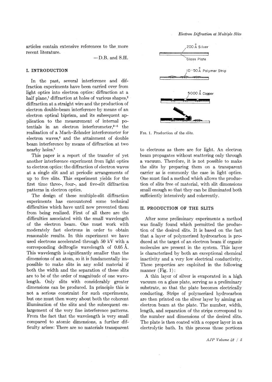
Electron Diffraction at Multiple Slits articles contain extensive references to the more 200 A Silver recent literature. -D.B.and S.H Glass Plate I.INTRODUCTION 10-50A Polymer Strip In the past,several interference and dif- fraction experiments have been carried over from light optics into electron optics:diffraction at a 5000 A Copper half plane,diffraction at holes of various shapes,? diffraction at a straight wire and the production of electron double-beam interference by means of an electron optical biprism,and its subsequent ap- plication to the measurement of internal po- tentials in an electron interferometer,3-5 the realization of a Mach-Zehnder interferometer for FIG.1.Production of the slits electron waves,and the attainment of double beam interference by means of diffraction at two nearby holes.7 to electrons as there are for light.An electron This paper is a report of the transfer of yet beam propagates without scattering only through another interference experiment from light optics a vacuum.Therefore,it is not possible to make to electron optics:the diffraction of electron waves the slits by preparing them on a transparent at a single slit and at periodic arrangements of carrier as is commonly the case in light optics. up to five slits.This experiment yields for the One must find a method which allows the produc- first time three-,four-,and five-slit diffraction tion of slits free of material,with slit dimensions patterns in electron optics. small enough so that they can be illuminated both The design of these multiple-slit diffraction sufficiently intensively and coherently. experiments has encountered some technical difficulties which have until now prevented them II.PRODUCTION OF THE SLITS from being realized.First of all there are the difficulties associated with the small wavelength After some preliminary experiments a method of the electron beam.One must work with was finally found which permitted the produc- moderately fast electrons in order to obtain tion of the desired slits.It is based on the fact reasonable results.In this experiment we have that a layer of polymerized hydrocarbon is pro- used electrons accelerated through 50 kV with a duced at the target of an electron beam if organic corresponding deBroglie wavelength of 0.05 A. molecules are present in the system.This layer This wavelength is significantly smaller than the is characterized by both an exceptional chemical dimensions of an atom,so it is fundamentally im- inactivity and a very low electrical conductivity. possible to make slits in any solid material if These properties are exploited in the following both the width and the separation of these slits manner (Fig.1): are to be of the order of magnitude of one wave- A thin layer of silver is evaporated in a high length.Only slits with considerably greater vacuum on a glass plate,serving as a preliminary dimensions can be produced.In principle this is substrate,so that the plate becomes electrically not a serious constraint for such experiments, conducting.Strips of polymerized hydrocarbon but one must then worry about both the coherent are then printed on the silver layer by aiming an illumination of the slits and the subsequent en- electron beam at the plate.The number,width, largement of the very fine interference patterns. length,and separation of the strips correspond to From the fact that the wavelength is very small the number and dimensions of the desired slits. compared to atomic dimensions,a further dif- The plate is then coated with a copper layer in an ficulty arises:There are no materials transparent electrolytic bath.In this process those portions AJP Volume 48 /5
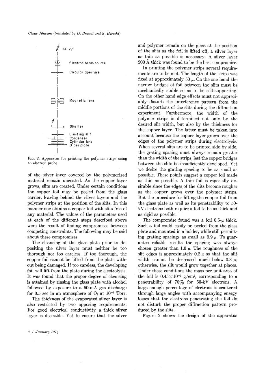
Claus Jonsson (translated by D.Brandt and S.Hirschi) and polymer remain on the glass at the position 40kV of the slits as the foil is lifted off,a silver layer as thin as possible is necessary.A silver layer Electron beam source 200 A thick was found to be the best compromise. In printing the polymer strips several require- Circular aperture ments are to be met.The length of the strips was fixed at approximately 50 4.On the one hand the narrow bridges of foil between the slits must be mechanically stable so as to be self-supporting. On the other hand edge effects must not appreci- Magnetic lens ably disturb the interference pattern from the middle portions of the slits during the diffraction experiment.Furthermore,the width of the polymer strips is determined not only by the Shutter desired slit width,but also by the thickness for the copper layer.The latter must be taken into Limiting slit Condenser account because the copper layer grows over the Cylinder lens edges of the polymer strips during electrolysis. Gloss plate When several slits are to be printed side by side, the grating spacing must always remain greater FIG.2.Apparatus for printing the polymer strips using than the width of the strips,lest the copper bridges an electron probe between the slits be insufficiently developed.Yet we desire the grating spacing to be as small as of the silver layer covered by the polymerized possible.These points suggest a copper foil made material remain uncoated.As the copper layer as thin as possible.A thin foil is especially de- grows,slits are created.Under certain conditions sirable since the edges of the slits become rougher the copper foil may be peeled from the glass as the copper grows over the polymer strips. carrier,leaving behind the silver layers and the But the procedure for lifting the copper foil from polymer strips at the position of the slits.In this the glass plate as well as its penetrability to 50- manner one obtains a copper foil with slits free of kV electrons both require a foil to be as thick and any material.The values of the parameters used as rigid as possible. at each of the different steps described above The compromise found was a foil 0.5-u thick. were the result of finding compromises between Such a foil could easily be peeled from the glass competing constraints.The following may be said plate and mounted in a holder,while still permitt- about these compromises. ing grating spacings as small as 0.9 g.To guar- The cleansing of the glass plate prior to de- antee reliable results the spacing was always positing the silver layer must neither be too chosen greater than 1.0 g.The roughness of the thorough nor too careless.If too thorough,the slit edges is approximately 0.2 so that the slit copper foil cannot be lifted from the plate with- width cannot be decreased much below 0.3 u; out being damaged.If too careless,the developing otherwise,the slit would grow together at places. foil will lift from the plate during the electrolysis. Under these conditions the mass per unit area of It was found that the proper degree of cleansing the foil is 0.45X10⁻³ g/cm2,corresponding to a is attained by rinsing the glass plate with alcohol penetrability of 70%for 50-kV electrons.A followed by exposure to a 50-mA gas discharge large enough percentage of electrons is scattered for 0.5 sec in an atmosphere of O2 at 10-*Torr. through large angles with accompanying energy The thickness of the evaporated silver layer is losses that the electrons penetrating the foil do also restricted by two opposing requirements. not disturb the proper diffraction pattern pro- For good electrical conductivity a thick silver duced by the slits. layer is desirable.Yet to ensure that the silver Figure 2 shows the design of the apparatus 6 January 197
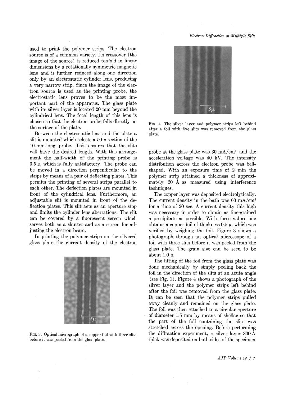
Electron Diffraction at Multiple Slits used to print the polymer strips.The electron source is of a common variety.Its crossover (the image of the source)is reduced tenfold in linear dimensions by a rotationally symmetric magnetic lens and is further reduced along one direction only by an electrostatic cylinder lens,producing a very narrow strip.Since the image of the elec- tron source is used as the printing probe,the electrostatic lens proves to be the most im- portant part of the apparatus.The glass plate with its silver layer is located 20 mm beyond the 5μ eylindrical lens.The focal length of this lens is chosen so that the electron probe falls directly on FIG.4.The silver layer and polymer strips left behind the surface of the plate. after a foil with five slits was removed from the glass Between the electrostatic lens and the plate a plate. slit is mounted which selects a 50-g section of the 10-mm-long probe.This ensures that the slits will have the desired length.With this arrange- probe at the glass plate was 30 mA/cm2,and the ment the half-width of the printing probe is acceleration voltage was 40 kV.The intensity 0.5 u,which is fully satisfactory.The probe can distribution across the electron probe was bell- be moved in.a direction perpendicular to the shaped.With an exposure time of 2 min the strips by means of a pair of deflecting plates.This polymer strip attained a thickness of approxi- permits the printing of several strips parallel to mately 20 A as measured using interference each other.The deflection plates are mounted in techniques. front of the cylindrical lens.Furthermore,an The copper layer was deposited electrolytically. adjustable slit is mounted in front of the de- The current density in the bath was 60 mA/cm2 flection plates.This slit acts as an aperture stop for a time of 20 sec.A current density this high and limits the cylinder lens aberrations.The slit was necessary in order to obtain as fine-grained can be covered by a fuorescent screen which a precipitate as possible.With these values one serves both as a shutter and as a screen for ad- obtains a copper foil of thickness 0.5 which was justing the electron beam. verified by weighing the foil.Figure 3 shows a In printing the polymer strips on the silvered photograph through an optical microscope of a glass plate the current density of the electron foil with three slits before it was peeled from the glass plate.The grain size can be seen to be about 1.0 u. The lifting of the foil from the glass plate was done mechanically by simply peeling back the foil in the direction of the slits at an acute angle (see Fig.1).Figure 4 shows a photograph of the silver layer and the polymer strips left behind after the foil was removed from the glass plate. It can be seen that the polymer strips pulled away cleanly and remained on the glass plate. The foil was then attached to a circular aperture of diameter 1.5 mm by means of shellac so that the part of the foil containing the slits was stretched across the opening.Before performing FIg.3.Optical micrograph of a copper foil with three slits the diffraction experiment,a silver layer 300 A before it was peeled from the glass plate. thick was deposited on both sides of the specimen AJP Volume 48 /7
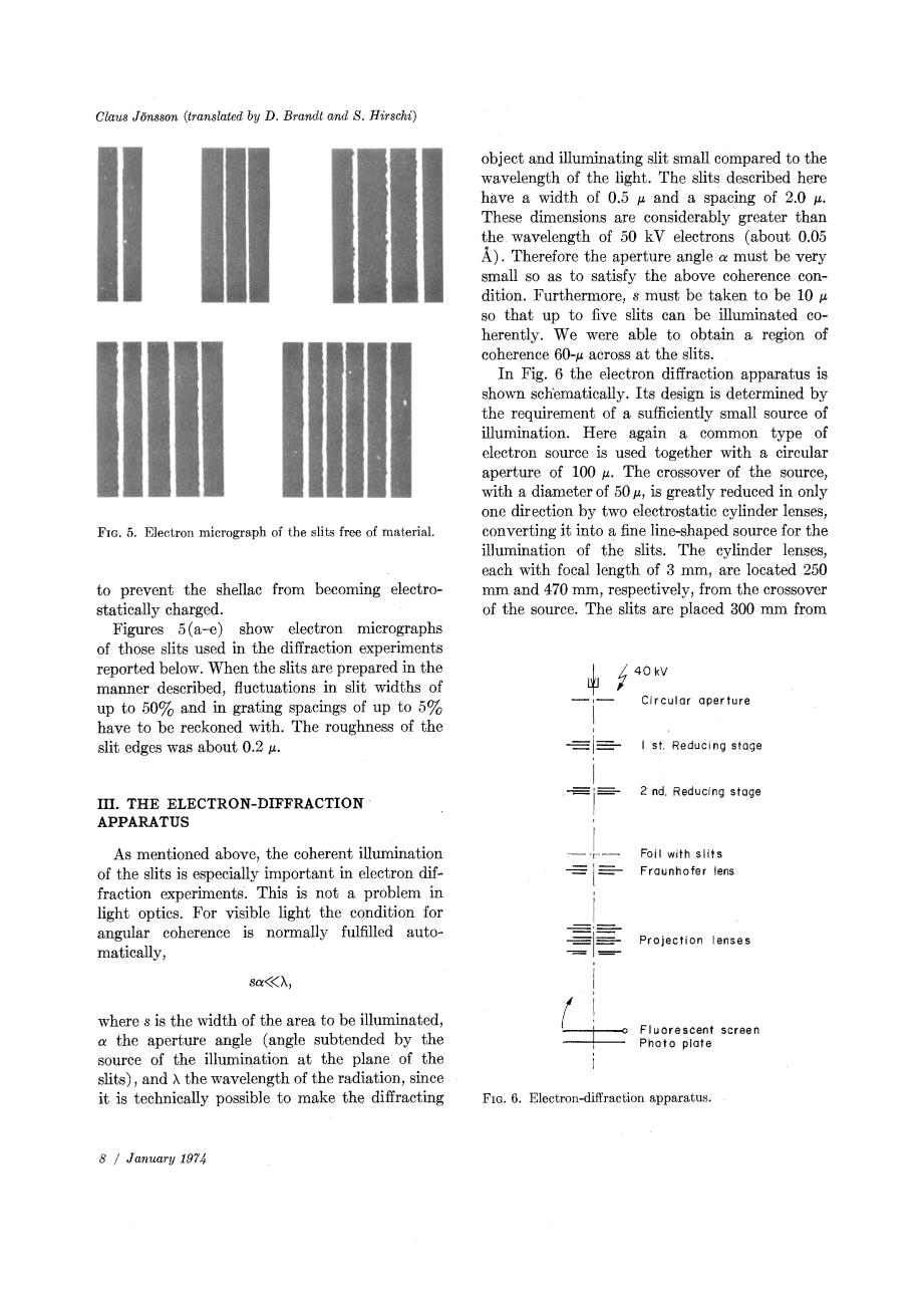
Ciaus Jonsson (translated by D.Brandt and S.Hirschi) object and illuminating slit small compared to the wavelength of the light.The slits described here have a width of 0.5 u and a spacing of 2.0 g. These dimensions are considerably greater than the wavelength of 50 kV electrons (about 0.05 A).Therefore the aperture angle a must be very small so as to satisfy the above coherence con- dition.Furthermore,s must be taken to be 10 u so that up to five slits can be illuminated co- herently.We were able to obtain a region of coherence 60-u across at the slits. In Fig.6 the electron diffraction apparatus is shown schematically.Its design is determined by the requirement of a sufficiently small source of illumination.Here again a common type of electron source is used together with a circular aperture of 100 u.The crossover of the source, with a diameter of 50u,is greatly reduced in only one direction by two electrostatic cylinder lenses, FIG.5.Electron micrograph of the slits free of material. converting it into a fine line-shaped source for the illumination of the slits.The cylinder lenses, each with focal length of 3 mm,are located 250 to prevent the shellac from becoming electro- mm and 470 mm,respectively,from the crossover statically charged. of the source.The slits are placed 300 mm from Figures 5(a-e)show electron micrographs of those slits used in the diffraction experiments reported below.When the slits are prepared in the manner described,fluctuations in slit widths of up to 50%and in grating spacings of up to 5% Circular aper ture have to be reckoned with.The roughness of the slit edges was about 0.2 u. 三岳 I st.Reducing stoge 三三 2 nd.Reducing stage II.THE ELECTRON-DIFFRACTION APPARATUS As mentioned above,the coherent illumination Foil with slits of the slits is especially important in electron dif- Fraunhofer lens fraction experiments.This is not a problem in light optics.For visible light the condition for angular coherence is normally fulfilled auto- Projection lenses matically, 8C<《入, where s is the width of the area to be illuminated, Fluorescent screen a the aperture angle (angle subtended by the Photo plate source of the illumination at the plane of the slits),and A the wavelength of the radiation,since it is technically possible to make the diffracting FIG.6.Electron-diffraction apparatus 8 January 1974