●●● ●●●● ●●●● ●●●● Function: ●●●● ●●●● ●●●● Transmitter:DA,PADA驱动放大,PA功放 ●● Receiver:LNA,high gain Amplifier 低噪声放大器,高增益放大器 Devices: Three-terminal solid-state device:BJT,FET,HBT, HEMT三端固态器件:双基晶体管,场效应管,HBT,HEMT Two-terminal solid-state device:Gunn,IMPATT 双端口固态器件:耿氏管,雪崩管 ●Microwave tube微波真空管 7
Three-terminal solid-state device: BJT, FET, HBT, HEMT三端固态器件:双基晶体管,场效应管, HBT, HEMT Two-terminal solid-state device: Gunn, IMPATT 双端口固态器件:耿氏管,雪崩管 Microwave tube 微波真空管 Transmitter: DA, PA DA驱动放大, PA功放 Receiver: LNA, high gain Amplifier 低噪声放大器,高增益放大器 Function: Devices: 7
●●】 ●●●● ●●●●● ●●●0 ●●●●0 ●●●● ●●●● §6.1 FET and BJT Models模型 ●● §6.2Two-port Power Gains双端口功率增益 §6.3.Stability稳定性 6.4 Amplifier Design using S Parameters 利用$参数进行放大器设计 6.5 Low-Noise Amplifier Design 1低噪声放大器 §6.6 Power Amplifier功放 8
§6.1 FET and BJT Models 模型 §6.2 Two-port Power Gains 双端口功率增益 §6.3. Stability 稳定性 §6.4 Amplifier Design using S Parameters 利用S参数进行放大器设计 §6.5 Low-Noise Amplifier Design 低噪声放大器 §6.6 Power Amplifier 功放 8
●●● ●●● ●●●● ●●●● ●●●● §6.1 FET and BJT Models ●●●0 Applications:Amplifier放大器,Oscillator振荡器,Switch 开关,Phase shifter移相器,Mixer混频器,Active filter有源滤 波器 Silicon bipolar device technology is mature and inexpensive,compared to Gaas transistor.与GaAs晶体 管相比,硅双基晶体管技术成熟且不贵。 ●Bipolar transistor:high gain高增益,high power capacity高功率容量,lower frequency工作频率低(<10GHz). ●GaAs FET:low noise figure,.低噪声系数much higher frequency工作于高频. 9
§6.1 FET and BJT Models Applications: Amplifier放大器, Oscillator振荡器, Switch 开关, Phase shifter移相器, Mixer混频器, Active filter有源滤 波器 Silicon bipolar device technology is mature and inexpensive, compared to GaAs transistor.与GaAs晶体 管相比,硅双基晶体管技术成熟且不贵。 Bipolar transistor: high gain高增益, high power capacity高功率容量, lower frequency 工作频率低(<10GHz). GaAs FET: low noise figure,低噪声系数 much higher frequency工作于高频. 9
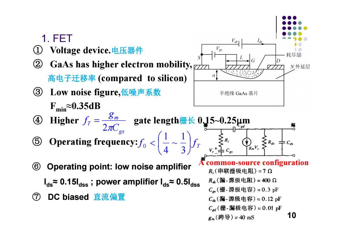
●●● ●●●● ●●●●● ●●●0 1.FET △。1●0 D● ① Voltage device.电压器件 )0 耗尽层 ② GaAs has higher electron mobility, D N外延层 高电子迁移率(compared to silicon) ③ Low noise figure,低噪声系数 半绝缘GaAs基片 Fmim≈0.35dB ④ Higher方= 8m nC. gate length栅长0,15~0.25um ⑤ Operating teequey: C ⑥ Operating point:low noise amplifier Acommon-source configuration R:(串联栅极电阻)=7D las≈0.15lass;power amplifier lds≈0.5ldss R.(漏-源极电阻)=4002 C,(栅-源极电容)=0.3pF ⑦ DC biased直流偏置 C.(漏-源极电容)=0.12pF Ca(栅-漏极电容)-0.01pF gm(跨导)-40mS 10
1. FET ⑥ Operating point: low noise amplifier Ids≈ 0.15Idss ; power amplifier Ids≈ 0.5Idss ⑦ DC biased 直流偏置 ① Voltage device.电压器件 ② GaAs has higher electron mobility, 高电子迁移率 (compared to silicon) ③ Low noise figure,低噪声系数 Fmin≈0.35dB gs m T C g f 2 ④ Higher gate length 栅长 0.15~0.25m T f f 31 ~ 41 ⑤ Operating frequency: 0 A common-source configuration 10
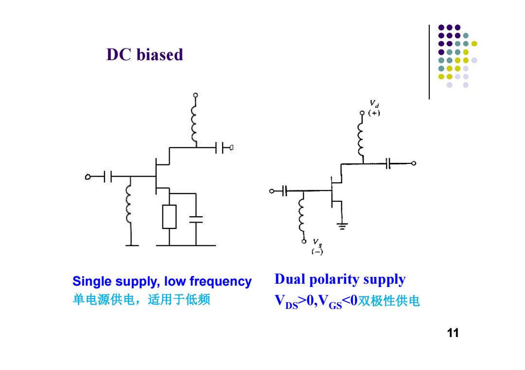
●●● ●●●● ●●●●@ DC biased ●●●0 ●●●●0 ●●●0 ●●●● ●● Single supply,low frequency Dual polarity supply 单电源供电,适用于低频 VDs>0,VGs<0双极性供电 11
Single supply, low frequency 单电源供电,适用于低频 Dual polarity supply VDS>0,VGS<0双极性供电 DC biased 11