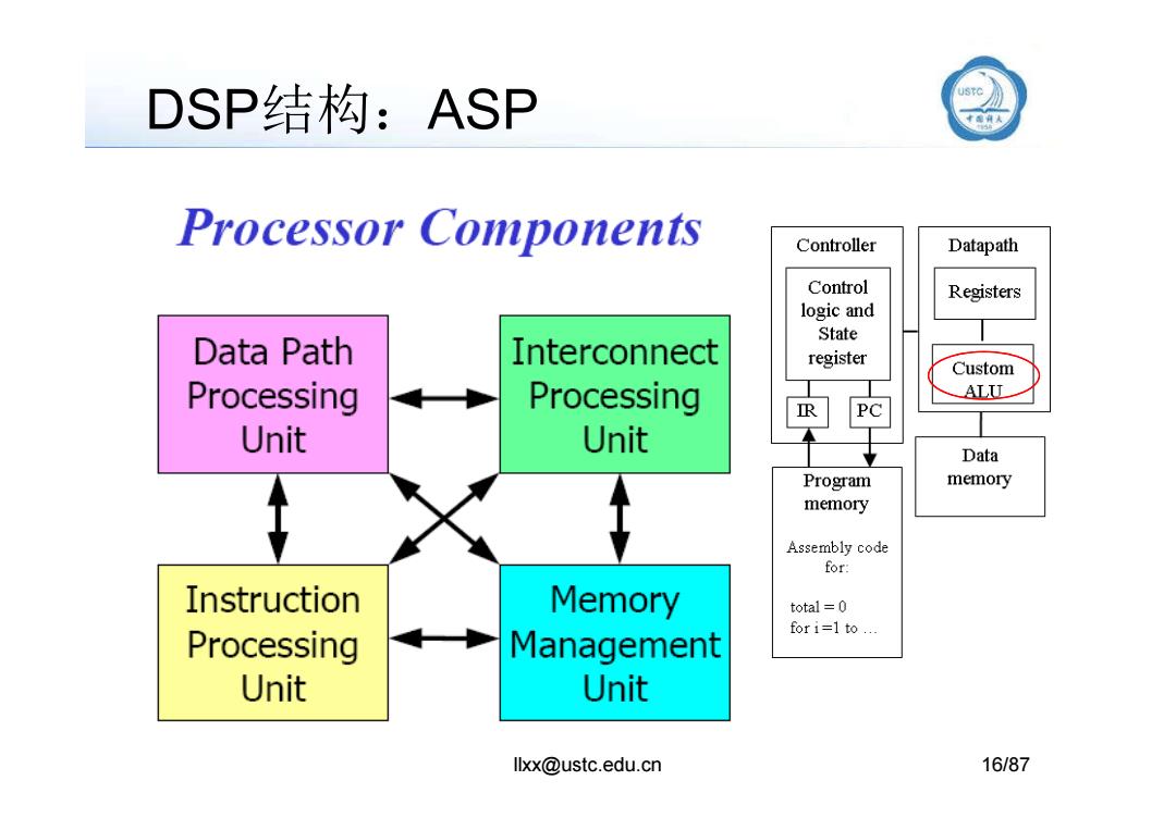
DSP结构:ASP e》 Processor Components Controller Datapath Control Registers logic and State Data Path Interconnect register Custom Processing Processing ALU Unit Unit Data Program memory memory Assembly code for: Instruction Memory total=0 fori=1 to... Processing Management Unit Unit llxx@ustc.edu.cn 16/87
DSP结构:ASP llxx@ustc.edu.cn 16/87
Characteristics of DSP's USTC CISC RISC Harvard One program fetch and multiple data R/W in each instruction cycle Multiple busses with restricted connectivity ·High l/O-rate Irregular register sets of different sizes Special purpose registers Special registers for zero-overhead loops 。 Multiply-add-accumulate in one instruction Single cycle multiply-accumulate (MAC) Fixed-point operations Hardware supported addressing modes Register indirect addressing with post-increment Bit-reversal addressing for FFT - Modulo addressing for hardware circular buffers Ilxx@ustc.edu.cn 17/87
Characteristics of DSP’s • CISC & RISC • Harvard – One program fetch and multiple data R/W in each instruction cycle • Multiple busses with restricted connectivity • High I/O-rate • Irregular register sets of different sizes • Special purpose registers llxx@ustc.edu.cn 17/87 • Special registers for zero-overhead loops • Multiply-add-accumulate in one instruction – Single cycle multiply-accumulate(MAC) • Fixed-point operations • Hardware supported addressing modes – Register indirect addressing with post-increment – Bit-reversal addressing for FFT – Modulo addressing for hardware circular buffers
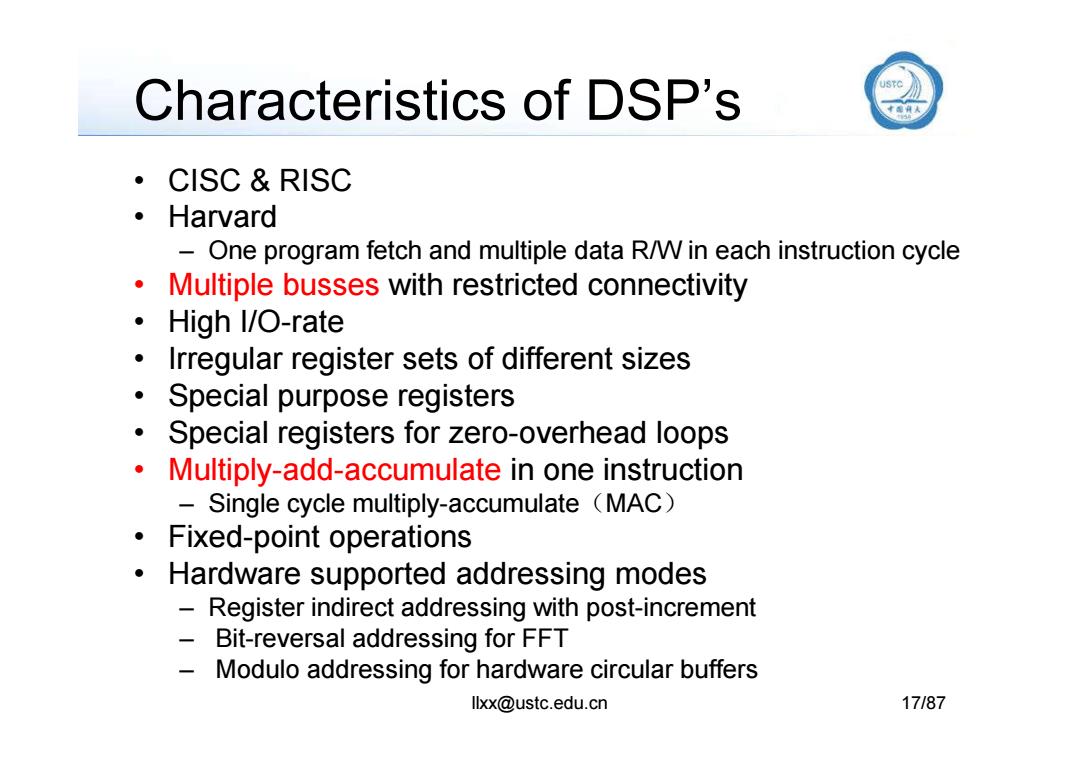
DSP的特殊指令 Sum-of-products operation for one data is executed in two cycles. General multiply processing also is executed in three cycles using a high-speed hardware multiplier. 80 40~70 bl6 70 A1 F(x)=∑C(n)*e x 60 2 A0 50 20~40 40 30 The high-speed 20 Hardware multiplier 9 10 47 2 1 -- bit:in HleG/ex C EC HCU C EC NCU M16g/60 M16g/0 DSP Without With M32C/83 multiplier multiplier
DSP的特殊指令 llxx@ustc.edu.cn 18/87
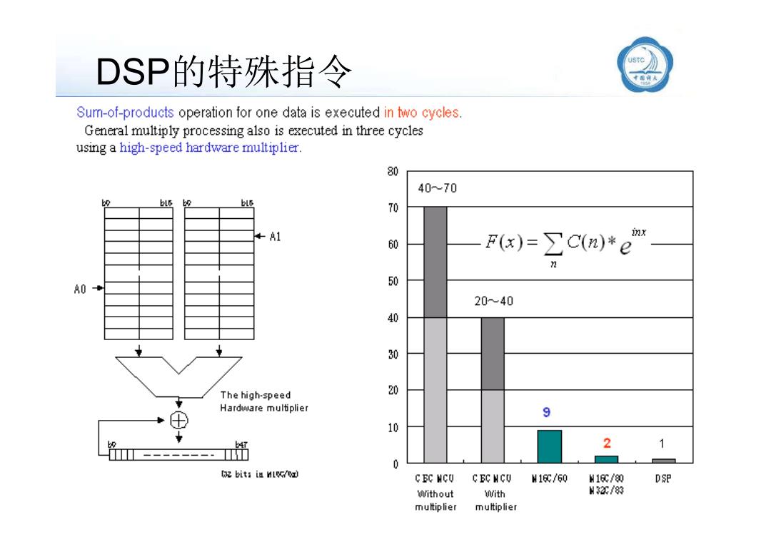
DSP的低功耗策略 》 P=Pam +Pse+P=0.5CLVDD'Af+IseVDD4+InVpD ·Power Management RISC User Defined Microprocessor Logic Gated clock Re-Configurable 1O DSP Power off un-used parts Logic RAM -Reduce clock rate of idle parts Variable Instruction Length Compressed Instruction Full-Custom Data Path Layout Technology and Voltage Scaling llxx@ustc.edu.cn 19/87
DSP的低功耗策略 • Power Management – Gated clock – Power off un-used parts dyn sc lk L DD sc DD lkVDD P P P P C V Af I V A I 2 0.5 llxx@ustc.edu.cn 19/87 – Reduce clock rate of idle parts • Variable Instruction Length • Compressed Instruction • Full-Custom Data Path Layout • Technology and Voltage Scaling
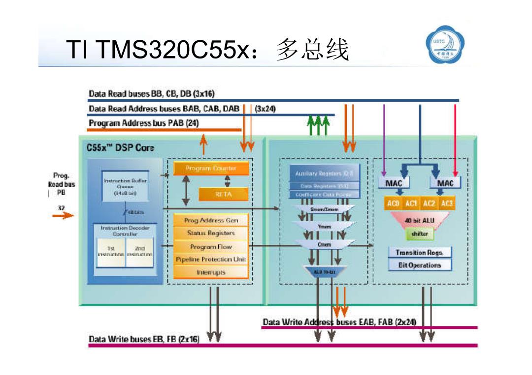
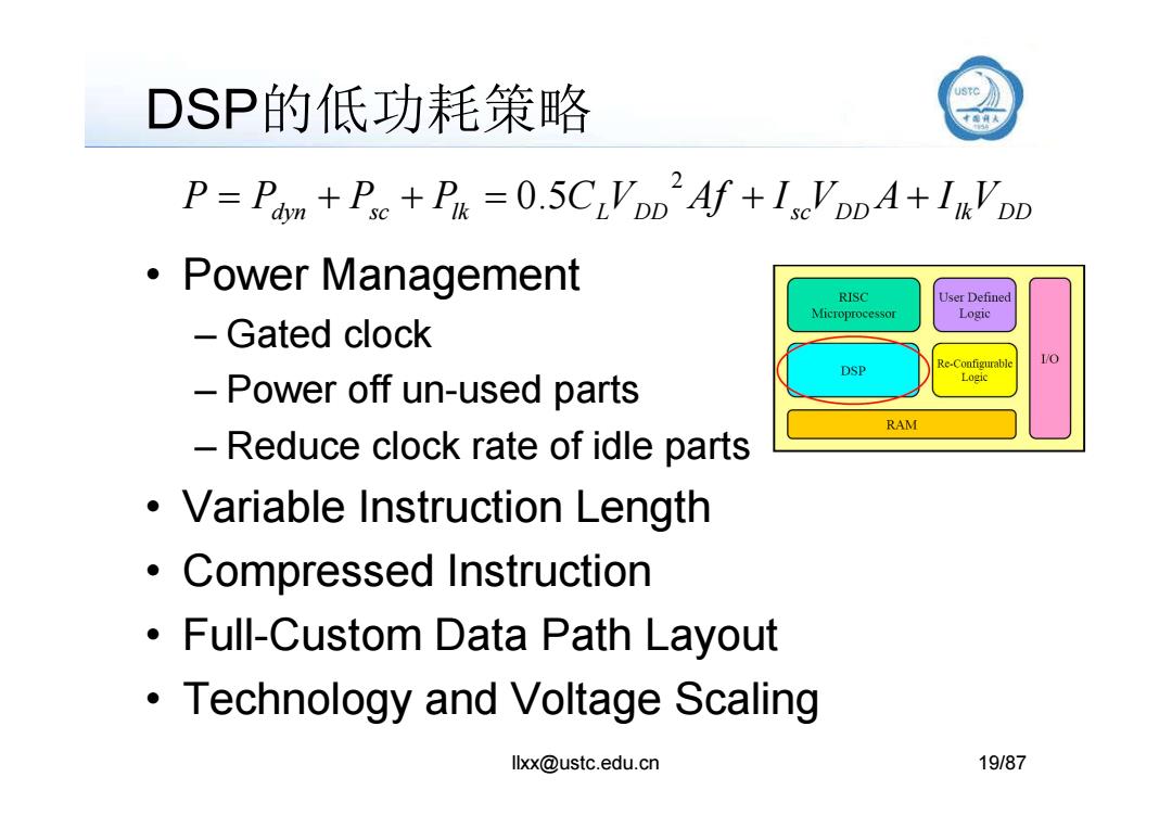
TI TMS320C55x:多总线 Data Read buses BB,CB,DB(3x16) Data Read Address buses BAB,CAB,DAB 3x24④ Program Address bus PAB(24) C55x"M DSP Core Prograr Ccuaiter Prog. Read bus MAC MAC PB (a4x060 A C0AC1AG2AC Prog Address Gen 40 bit ALU Irminction Deceder Siatus Registers shiter 2nd Program Fow ngnctce Transtion Rogs. Pipeline Protecticn Unit Bit Operations hterrupis Data Write Addrest buses EAB.FAB(2x24) Data Write buses EB.FB 2x16) 7
TI TMS320C55x:多总线 llxx@ustc.edu.cn 20/87