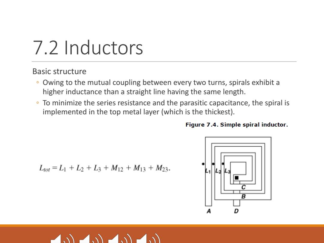
7.2 Inductors Basic structure Owing to the mutual coupling between every two turns,spirals exhibit a higher inductance than a straight line having the same length. To minimize the series resistance and the parasitic capacitance,the spiral is implemented in the top metal layer (which is the thickest). Figure 7.4.Simple spiral inductor. Lom=L1+L2+L3+M12+M13+M23 D
7.2 Inductors Basic structure ◦ Owing to the mutual coupling between every two turns, spirals exhibit a higher inductance than a straight line having the same length. ◦ To minimize the series resistance and the parasitic capacitance, the spiral is implemented in the top metal layer (which is the thickest)
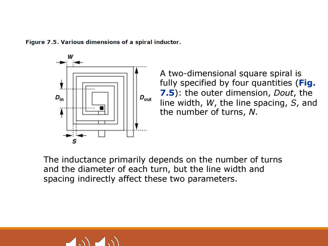
Figure 7.5.Various dimensions of a spiral inductor. A two-dimensional square spiral is fully specified by four quantities (Fig. Dout 7.5):the outer dimension,Dout,the line width,W,the line spacing,S,and the number of turns,N. The inductance primarily depends on the number of turns and the diameter of each turn,but the line width and spacing indirectly affect these two parameters
A two-dimensional square spiral is fully specified by four quantities (Fig. 7.5): the outer dimension, Dout, the line width, W, the line spacing, S, and the number of turns, N. The inductance primarily depends on the number of turns and the diameter of each turn, but the line width and spacing indirectly affect these two parameters
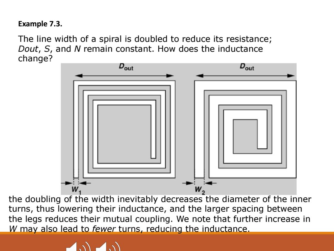
Example 7.3. The line width of a spiral is doubled to reduce its resistance; Dout,S,and N remain constant.How does the inductance change? Dout Dout Wj W2 the doubling of the width inevitably decreases the diameter of the inner turns,thus lowering their inductance,and the larger spacing between the legs reduces their mutual coupling.We note that further increase in W may also lead to fewer turns,reducing the inductance
Example 7.3. The line width of a spiral is doubled to reduce its resistance; Dout, S, and N remain constant. How does the inductance change? the doubling of the width inevitably decreases the diameter of the inner turns, thus lowering their inductance, and the larger spacing between the legs reduces their mutual coupling. We note that further increase in W may also lead to fewer turns, reducing the inductance

Compared with transistors and resistors,inductors typically have much greater dimensions ("foot prints"),resulting in a large chip area and long interconnects traveling from one block to another.It is therefore desirable to minimize the outer dimensions of inductors. Figure 7.7.Effect of(a)reducing the outer dimension and the line width,or(b)reducing the outer dimension and increasing the number of turns. [View full size imagel Dout2 Dout2 (a) (b) the line resistance the mutual coupling rises,degrading the between the sides inductor quality of the innermost turns reduces the inductance
Compared with transistors and resistors, inductors typically have much greater dimensions (“foot prints”), resulting in a large chip area and long interconnects traveling from one block to another. It is therefore desirable to minimize the outer dimensions of inductors. the line resistance rises, degrading the inductor quality the mutual coupling between the sides of the innermost turns reduces the inductance
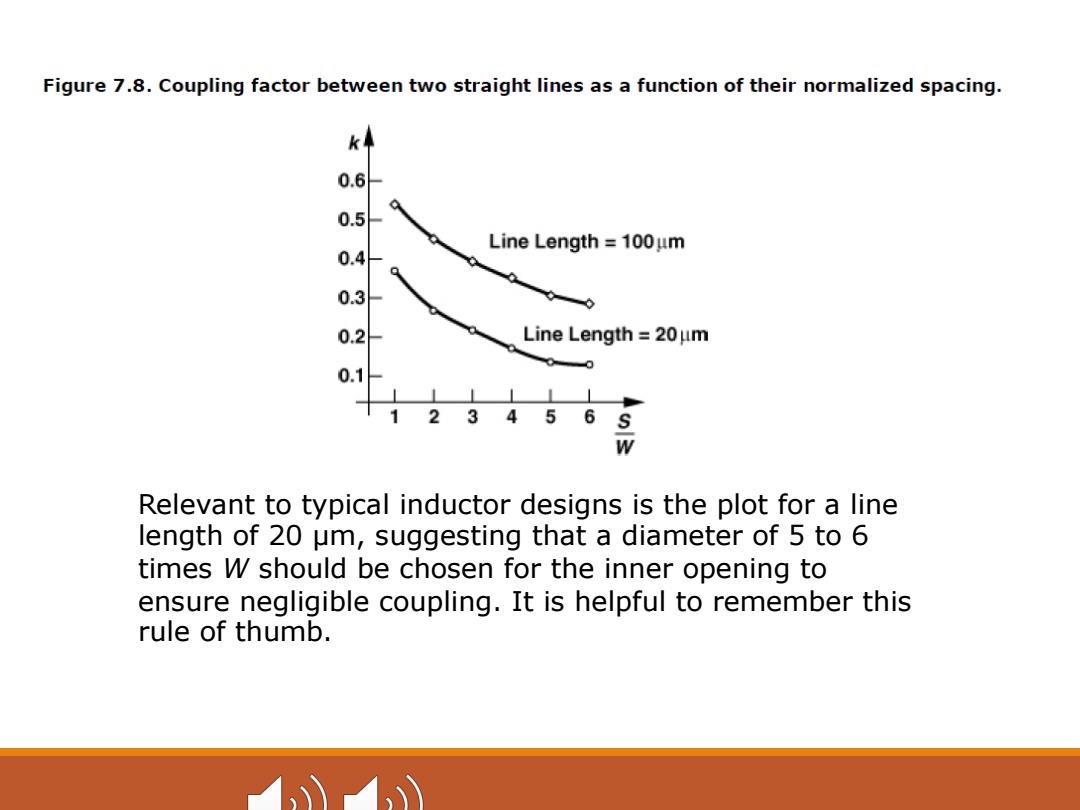
Figure 7.8.Coupling factor between two straight lines as a function of their normalized spacing. k 0.6 0.5 Line Length =100um 0.4 0.3 0.2 Line Length=20μm 0-0 0.1 123456S W Relevant to typical inductor designs is the plot for a line length of 20 um,suggesting that a diameter of 5 to 6 times W should be chosen for the inner opening to ensure negligible coupling.It is helpful to remember this rule of thumb
Relevant to typical inductor designs is the plot for a line length of 20 µm, suggesting that a diameter of 5 to 6 times W should be chosen for the inner opening to ensure negligible coupling. It is helpful to remember this rule of thumb