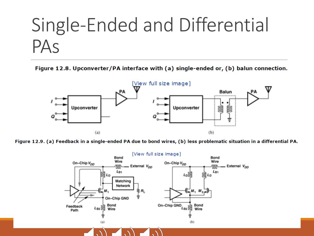
Single-Ended and Differential PAS Figure 12.8.Upconverter/PA interface with (a)single-ended or,(b)balun connection. View full size image] Balun Upconverter Upconverter (a) (b) Figure 12.9.(a)Feedback in a single-ended PA due to bond wires,(b)less problematic situation in a differential PA. [View full size image] Bond Bond On-Chip Voo Wire On-Chip Voo Wire 00 External Vpo 00一External Voo L81 LB1 Lo L02 L Matching Network On-Chip GND Feedback On-Chip GND Bond Path LBond Wire L823 Wire a
Single-Ended and Differential PAs

Single-Ended and Differential PAS Figure 12.10.Use of a balun between the PA and antenna. Balun PA Upconverter Suppose a given balun design has a loss of 1.5 dB.In which one of the transmitters shown in Figs.12.8(b)and 12.10 does this loss affect the efficiency more adversely? 30 dBm output compared to 0 dBm input 300 mW compared to 0.3 mW
Single-Ended and Differential PAs Suppose a given balun design has a loss of 1.5 dB. In which one of the transmitters shown in Figs. 12.8(b) and 12.10 does this loss affect the efficiency more adversely? 30 dBm output compared to 0 dBm input 300 mW compared to 0.3 mW
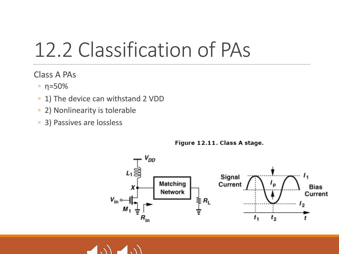
12.2 Classification of PAs Class A PAs 。n=50% 1)The device can withstand 2 VDD 2)Nonlinearity is tolerable 3)Passives are lossless Figure 12.11.Class A stage. VpD Signal X Matching Current Bias Network Current Vin 李R 12 M1吉 0 1? t
12.2 Classification of PAs Class A PAs ◦ η=50% ◦ 1) The device can withstand 2 VDD ◦ 2) Nonlinearity is tolerable ◦ 3) Passives are lossless
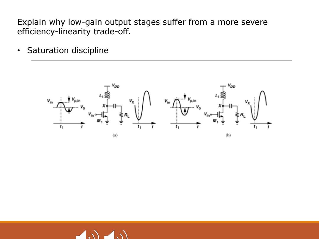
Explain why low-gain output stages suffer from a more severe efficiency-linearity trade-off. Saturation discipline VDD (b)
Explain why low-gain output stages suffer from a more severe efficiency-linearity trade-off. • Saturation discipline

Efficiency boosting for class-A PAS (1)the supply voltage and bias current remain at the levels necessary for full output power and only the input signal swing is reduced Output power Full output power Equation 12.17,12.18 2/(2Rm) [VBD/(2Rm】 V2/(2Rm) 01= DC supply voltage Vop/Rin VDD DC supply current Satisfying the full power VDD/Rin
Efficiency boosting for class-A PAs (1) the supply voltage and bias current remain at the levels necessary for full output power and only the input signal swing is reduced Output power Full output power DC supply voltage �!! DC supply current Satisfying the full power �!!/�"#