
UNISONIC TECHNOLOGIES CO.,LTD 8N60 Power MOSFET 7.5 Amps,600/650 Volts N-CHANNEL POWER MOSFET ■DESCRIPTION TO-220 The UTC 8N60 is a high voltage and high current power MOSFET,designed to have better characteristics,such as fast switching time,low gate charge,low on-state resistance and have a high rugged avalanche characteristics.This power MOSFET is usually used at high speed switching applications in power supplies,PWM motor controls,high efficient DC to DC converters TO-220F and bridge circuits. ■FEATURES *Pb-free plating product number:8N60L *RDS(ON)=1.2Q @VGs=10V Ultra low gate charge(typical 28 nc *Low reverse transfer capacitance(CRss=typical 12.0 pF *Fast switching capability *Avalanche energy specified *Improved dv/dt capability,high ruggedness SYMBOL 2.Drain 1.Gate 3.Source ORDERING INFORMATION Ordering Number Pin Assignment Package Normal Lead Free Plating 123 Packing 8N60-x-TA3-T 8N60L-x-TA3-T T0-220 Tube 8N60-x-TF3-T 8N60L-x-TF3-T TO-220F G Tube 8N60L-X-TA3-T (1)Packing Type (1)T:Tube (2)Package Type (2)TA3:T0-220,TF3:T0-220F (3)Drain-Source Vollage (3)A600V,B:650V (4)Lead Plating (4)L:Lead Free Plating,Blank:Pb/Sn www.unisonic.com.tw 1 of8 Copyright@2007 Unisonic Technologies Co.,Ltd QW-R502-115.B
UNISONIC TECHNOLOGIES CO., LTD 8N60 Power MOSFET www.unisonic.com.tw 1 of 8 Copyright © 2007 Unisonic Technologies Co., Ltd QW-R502-115,B 7.5 Amps, 600/650 Volts N-CHANNEL POWER MOSFET DESCRIPTION The UTC 8N60 is a high voltage and high current power MOSFET, designed to have better characteristics, such as fast switching time, low gate charge, low on-state resistance and have a high rugged avalanche characteristics. This power MOSFET is usually used at high speed switching applications in power supplies, PWM motor controls, high efficient DC to DC converters and bridge circuits. FEATURES * RDS(ON) = 1.2Ω @VGS = 10 V * Ultra low gate charge ( typical 28 nC ) * Low reverse transfer capacitance ( CRSS = typical 12.0 pF ) * Fast switching capability * Avalanche energy specified * Improved dv/dt capability, high ruggedness SYMBOL 1.Gate 3.Source 2.Drain *Pb-free plating product number: 8N60L ORDERING INFORMATION Ordering Number Pin Assignment Normal Lead Free Plating Package 1 2 3 Packing 8N60-x-TA3-T 8N60L-x-TA3-T TO-220 G D S Tube 8N60-x-TF3-T 8N60L-x-TF3-T TO-220F G D S Tube

8N60 Power MOSFET ABSOLUTE MAXIMUM RATINGS (Tc=25C,unless otherwise specified) PARAMETER SYMBOL RATINGS UNIT Drain-Source Voltage 8N60-A 8N60-B Voss 600 V 650 V Gate-Source Voltage VGss ±30 V Avalanche Current (Note 1) IAR 7.5 A Tc=25°C 7.5 Continuous Drain Current A Tc=100C lo 4.6 A Pulsed Drain Current(Note 1) IDM 30 A Single Pulsed (Note 2) EAS 230 mJ Avalanche Energy Repetitive(Note 1) EAR 14.7 mJ Peak Diode Recovery dv/dt(Note 3) dv/dt 4.5 V/ns T0-220 147 W Power Dissipation TO-220F Po 48 W Junction Temperature T +150 ℃ Operating Temperature ToPR -55~+150 ℃ Storage Temperature TsTG -55~+150 ℃ Note:Absolute maximum ratings are those values beyond which the device could be permanently damaged. Absolute maximum ratings are stress ratings only and functional device operation is not implied. ■ THERMAL DATA PARAMETER SYMBOL RATING UNIT Junction-to-Ambient T0-220 62.5 CN TO-220F BJA 62.5 CN Junction-to-Case T0-220 0.85 CN Bsc TO-220F 2.6 CM ELECTRICAL CHARACTERISTICS(Tc=25C,unless otherwise specified) PARAMETER SYMBOL TEST CONDITIONS MINTYP MAX UNIT OFF CHARACTERISTICS Drain-Source Breakdown Voltage 8N60-A 8N60-B BVpss 600 V Vcs=0V,lb=250μA 650 V Drain-Source Leakage Current Ipss Vps=600 V.VGs=0V 10 uA Gate-Source Leakage Current Forward VGs 30 V.Vos =0V 100nA Reverse lGss Ves =-30 V,VDs=0V -100nA Breakdown Voltage Temperature △BVos△T) lp=250 uA,Referenced to 25C 0.7 VrC Coefficient ON CHARACTERISTICS Gate Threshold Voltage VGS(TH) Vos VGs,ID 250 JA 2.0 4.0V Static Drain-Source On-State Resistance RDS(ON) VGs 10 V,Ip =3.75 A 1.01.20 DYNAMIC CHARACTERISTICS Input Capacitance Ciss 9651255pF Output Capacitance Coss Vos=25V.VGs=0V.f=1MHz 105135pF Reverse Transfer Capacitance CRSS 12 16 pF SWITCHING CHARACTERISTICS Turn-On Delay Time tp(ON) 16.545ns Turn-On Rise Time VoD=300V,lb=7.5A,RG=250 60.5130ns Turn-Off Delay Time tD(OFF) (Note 4.5) 81170ns Turn-Off Fall Time tE 64.5140ns Total Gate Charge QG 2836nC Gate-Source Charge QGs VDs=480V,lD=7.5A,VGs=10V (Note 4.5) 4.5 nC Gate-Drain Charge QGD 12 nC UIC UNISONIC TECHNOLOGIES CO,LTD 2 of 8 www.unisonic.com.tw QW-R502-115.B
8N60 Power MOSFET UNISONIC TECHNOLOGIES CO., LTD 2 of 8 www.unisonic.com.tw QW-R502-115,B ABSOLUTE MAXIMUM RATINGS (TC = 25℃, unless otherwise specified) PARAMETER SYMBOL RATINGS UNIT 8N60-A 600 V Drain-Source Voltage 8N60-B VDSS 650 V Gate-Source Voltage VGSS ±30 V Avalanche Current (Note 1) IAR 7.5 A TC = 25°C 7.5 A Continuous Drain Current TC = 100°C ID 4.6 A Pulsed Drain Current (Note 1) IDM 30 A Single Pulsed (Note 2) EAS 230 mJ Avalanche Energy Repetitive (Note 1) EAR 14.7 mJ Peak Diode Recovery dv/dt (Note 3) dv/dt 4.5 V/ns TO-220 147 W Power Dissipation TO-220F PD 48 W Junction Temperature TJ +150 ℃ Operating Temperature TOPR -55 ~ +150 ℃ Storage Temperature TSTG -55 ~ +150 ℃ Note: Absolute maximum ratings are those values beyond which the device could be permanently damaged. Absolute maximum ratings are stress ratings only and functional device operation is not implied. THERMAL DATA PARAMETER SYMBOL RATING UNIT TO-220 62.5 °C/W Junction-to-Ambient TO-220F θJA 62.5 °C/W TO-220 0.85 °C/W Junction-to-Case TO-220F θJC 2.6 °C/W ELECTRICAL CHARACTERISTICS (TC =25℃, unless otherwise specified) PARAMETER SYMBOL TEST CONDITIONS MIN TYP MAX UNIT OFF CHARACTERISTICS 8N60-A 600 V Drain-Source Breakdown Voltage 8N60-B BVDSS VGS = 0 V, ID = 250 µA 650 V Drain-Source Leakage Current IDSS VDS = 600 V, VGS = 0 V 10 µA Forward VGS = 30 V, VDS = 0 V 100 nA Gate-Source Leakage Current Reverse IGSS VGS = -30 V, VDS = 0 V -100 nA Breakdown Voltage Temperature Coefficient △BVDSS/△TJ ID = 250 µA, Referenced to 25°C 0.7 V/℃ ON CHARACTERISTICS Gate Threshold Voltage VGS(TH) VDS = VGS, ID = 250 µA 2.0 4.0 V Static Drain-Source On-State Resistance RDS(ON) VGS = 10 V, ID = 3.75 A 1.0 1.2 Ω DYNAMIC CHARACTERISTICS Input Capacitance CISS 965 1255 pF Output Capacitance COSS 105 135 pF Reverse Transfer Capacitance CRSS VDS = 25 V, VGS = 0 V, f = 1MHz 12 16 pF SWITCHING CHARACTERISTICS Turn-On Delay Time tD(ON) 16.5 45 ns Turn-On Rise Time tR 60.5 130 ns Turn-Off Delay Time tD(OFF) 81 170 ns Turn-Off Fall Time tF VDD = 300V, ID = 7.5 A, RG = 25Ω (Note 4, 5) 64.5 140 ns Total Gate Charge QG 28 36 nC Gate-Source Charge QGS 4.5 nC Gate-Drain Charge QGD VDS= 480V,ID= 7.5A, VGS= 10 V (Note 4, 5) 12 nC

8N60 Power MOSFET ◆ ELECTRICAL CHARACTERISTICS(Cont.) PARAMETER SYMBOL TEST CONDITIONS MIN TYP MAX UNIT DRAIN-SOURCE DIODE CHARACTERISTICS AND MAXIMUM RATINGS Drain-Source Diode Forward Voltage Ves =0 V,Is =7.5 A 1.4V Maximum Continuous Drain-Source Diode 7.5 Forward Current Is A Maximum Pulsed Drain-Source Diode 30 Forward Current IsM A Reverse Recovery Time tRR Ves =0V,Is =7.5 A. 365 ns Reverse Recovery Charge ORR dl-/dt=100 A/us (Note 4) 3.4 μC Notes:1.Repetitive Rating:Pulse width limited by TJ 2.L=7.3mH,IAs 7.5A,VDD=50V,RG=25 Q,Starting TJ=25C 3.lso≤7.5A,di/dts200AWμs,Voo≤BVpss,.Starting TJ=25℃ 4.Pulse Test:Pulse width s 300us,Duty cycle s2% 5.Essentially independent of operating temperature UIC UNISONIC TECHNOLOGIES CO.,LTD 3 of 8 www.unisonic.com.tw QW-R502-115.B
8N60 Power MOSFET UNISONIC TECHNOLOGIES CO., LTD 3 of 8 www.unisonic.com.tw QW-R502-115,B ELECTRICAL CHARACTERISTICS(Cont.) PARAMETER SYMBOL TEST CONDITIONS MIN TYP MAX UNIT DRAIN-SOURCE DIODE CHARACTERISTICS AND MAXIMUM RATINGS Drain-Source Diode Forward Voltage VSD VGS = 0 V, IS = 7.5 A 1.4 V Maximum Continuous Drain-Source Diode Forward Current IS 7.5 A Maximum Pulsed Drain-Source Diode Forward Current ISM 30 A Reverse Recovery Time tRR 365 ns Reverse Recovery Charge QRR VGS = 0 V, IS = 7.5 A, dIF/dt = 100 A/µs (Note 4) 3.4 µC Notes: 1. Repetitive Rating : Pulse width limited by TJ 2. L = 7.3mH, IAS = 7.5A, VDD = 50V, RG = 25 Ω, Starting TJ = 25°C 3. ISD ≤ 7.5A, di/dt ≤200A/µs, VDD ≤ BVDSS, Starting TJ = 25°C 4. Pulse Test: Pulse width ≤ 300µs, Duty cycle ≤ 2% 5. Essentially independent of operating temperature
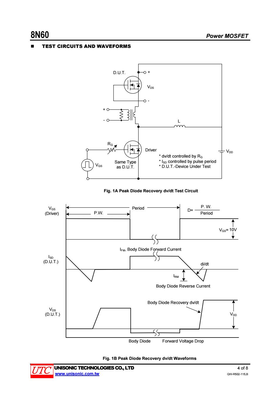
8N60 Power MOSFET TEST CIRCUITS AND WAVEFORMS D.U.T. 0+ Vos 01 L Driver dv/dt controlled by R Same Type *Isp controlled by pulse period as D.U.T. *D.U.T.-Device Under Test Fig.1A Peak Diode Recovery dv/dt Test Circuit Ves Period P.W. D=- (Driver) P.W. Period VGs=10V IFM.Body Diode Forward Current Isp (D.U.T.) di/dt IRM Body Diode Reverse Current Body Diode Recovery dv/dt Vos (D.U.T.) Body Diode Forward Voltage Drop Fig.1B Peak Diode Recovery dv/dt Waveforms UIC UNISONIC TECHNOLOGIES CO.,LTD 4 of8 www.unisonic.com.tw QW-R502-115.B
8N60 Power MOSFET UNISONIC TECHNOLOGIES CO., LTD 4 of 8 www.unisonic.com.tw QW-R502-115,B TEST CIRCUITS AND WAVEFORMS Same Type as D.U.T. L VDD Driver VGS RG - VDS D.U.T. + * dv/dt controlled by RG * ISD controlled by pulse period * D.U.T.-Device Under Test P. W. Period D= VGS (Driver) ISD (D.U.T.) IFM, Body Diode Forward Current di/dt IRM Body Diode Reverse Current Body Diode Recovery dv/dt Body Diode Forward Voltage Drop VDD 10V VDS (D.U.T.) - + VGS= P.W. Period Fig. 1A Peak Diode Recovery dv/dt Test Circuit Fig. 1B Peak Diode Recovery dv/dt Waveforms

8N60 Power MOSFET TEST CIRCUITS AND WAVEFORMS(Cont.) R Vos Vos 90% Voo w 10% 王10N D.U.T. Fig.2A Switching Test Circuit Fig.2B Switching Waveforms Vas Same Type I as D.U.T. Q 0.2f 0.34F 10V 卡Vbs -Qs→ —QGD Q DUT 3mA几 Charge Fig.3A Gate Charge Test Circuit Fig.3B Gate Charge Waveform Vos BVpss IAS VoD 10V 几 D.U.T Time Fig.4A Unclamped Inductive Switching Test Circuit Fig.4B Unclamped Inductive Switching Waveforms UIC UNISONIC TECHNOLOGIES CO.,LTD 5 of 8 www.unisonic.com.tw QW-R502-115.B
8N60 Power MOSFET UNISONIC TECHNOLOGIES CO., LTD 5 of 8 www.unisonic.com.tw QW-R502-115,B TEST CIRCUITS AND WAVEFORMS (Cont.) Fig. 2A Switching Test Circuit Fig. 2B Switching Waveforms Fig. 3A Gate Charge Test Circuit Fig. 3B Gate Charge Waveform D.U.T. RD 10V VDS L VDD tp VDD tp Time BVDSS IAS ID(t) VDS(t) Fig. 4A Unclamped Inductive Switching Test Circuit Fig. 4B Unclamped Inductive Switching Waveforms