
Stability the LNA must remain stable for all source impedances at all frequencies. One may think that the LNA must operate properly only in the frequency band of interest and not necessarily at other frequencies,but if the LNA begins to oscillate at any frequency,it becomes highly nonlinear and its gain is very heavily compressed. 1+1△2-1S112-1S222 2S21S12
Stability the LNA must remain stable for all source impedances at all frequencies. One may think that the LNA must operate properly only in the frequency band of interest and not necessarily at other frequencies, but if the LNA begins to oscillate at any frequency, it becomes highly nonlinear and its gain is very heavily compressed
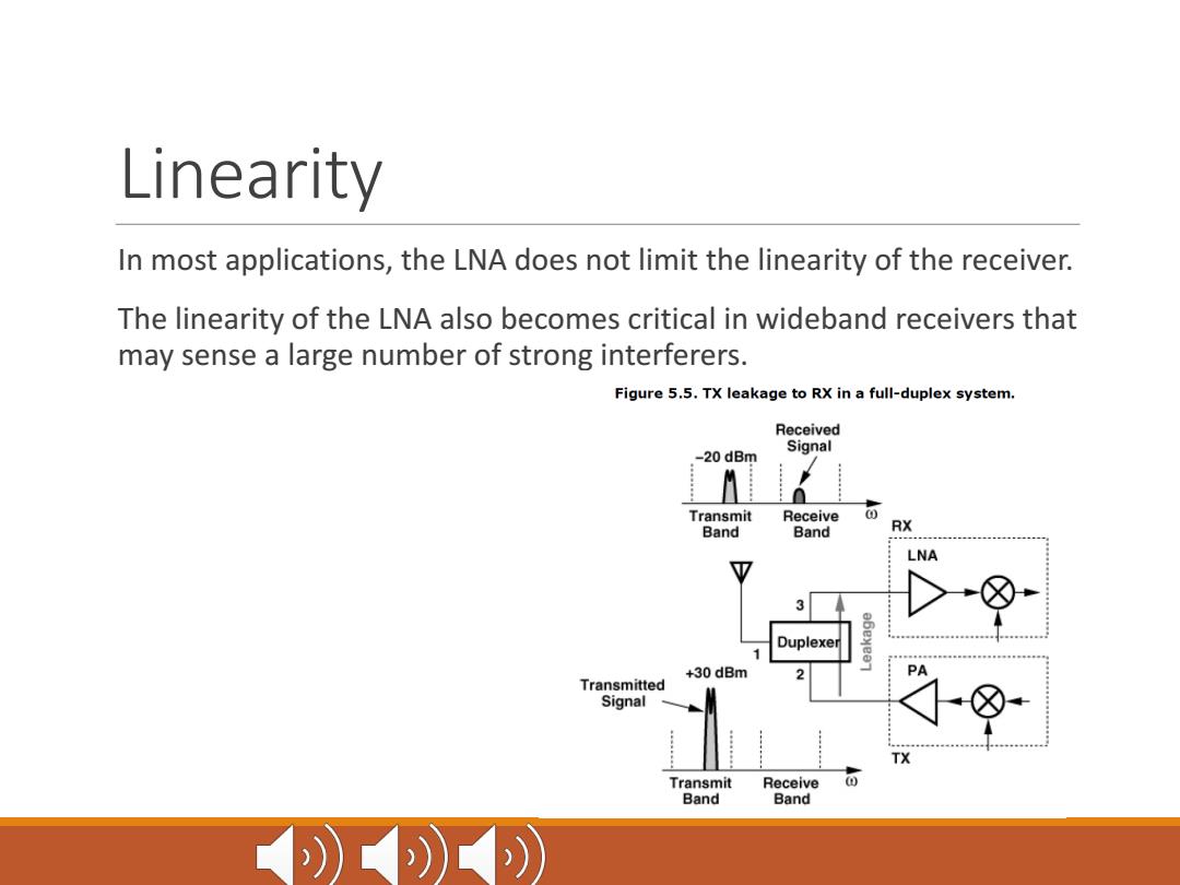
Linearity In most applications,the LNA does not limit the linearity of the receiver. The linearity of the LNA also becomes critical in wideband receivers that may sense a large number of strong interferers. Figure 5.5.TX leakage to RX in a full-duplex system. Received -20 dBm Signal Transmit Receive Band Band RX LNA 3 Duplexer +30 dBm Transmitted Signal TX Transmit Receive Band Band )))
Linearity In most applications, the LNA does not limit the linearity of the receiver. The linearity of the LNA also becomes critical in wideband receivers that may sense a large number of strong interferers
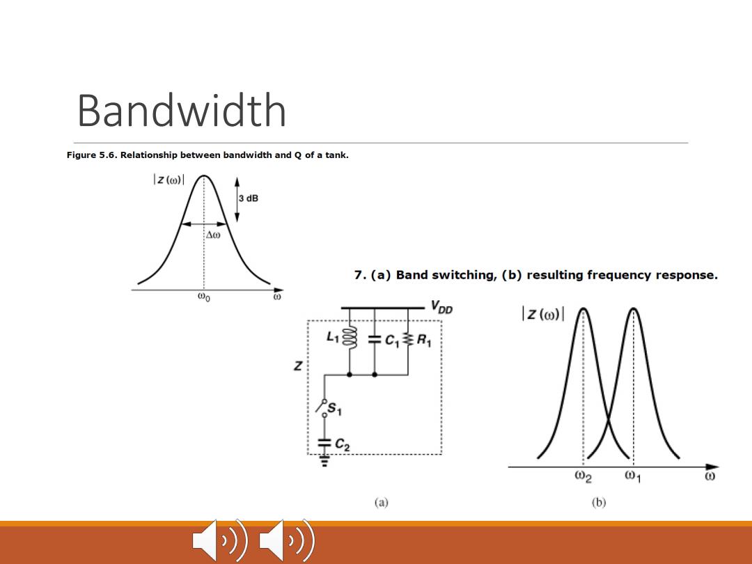
Bandwidth Figure 5.6.Relationship between bandwidth and Q of a tank. z(o川 3 dB △0 7.(a)Band switching,(b)resulting frequency response. 00 VoD 1Z(o)川 L1意卡CR1 2 01 (a) (b) K
Bandwidth
Power Dissipation The LNA typically exhibits a direct trade-off among noise,linearity,and power dissipation. Nonetheless,in most receiver designs,the LNA consumes only a small fraction of the overall power. In other words,the circuit's noise figure generally proves much more critical than its power dissipation
Power Dissipation The LNA typically exhibits a direct trade-off among noise, linearity, and power dissipation. Nonetheless, in most receiver designs, the LNA consumes only a small fraction of the overall power. In other words, the circuit’s noise figure generally proves much more critical than its power dissipation
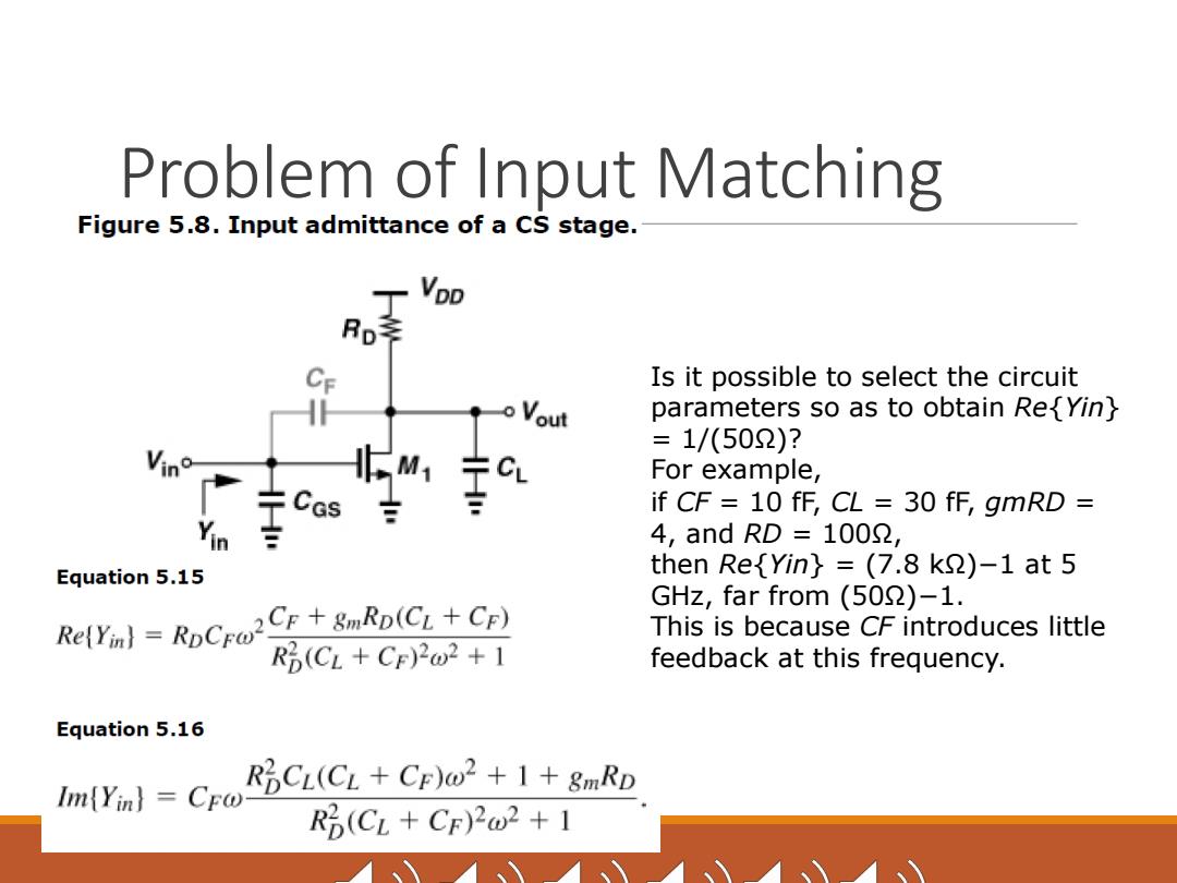
Problem of Input Matching Figure 5.8.Input admittance of a CS stage. Rp Is it possible to select the circuit o Vout parameters so as to obtain Re{yin} =1/(502)? CL For example, GS if CF 10 fF,CL 30 fF,gmRD in 4,and RD=1002, Equation 5.15 then Re{Yin}=(7.8 k)-1 at 5 Re(Ym)=RpCro2Cr+gmRp(CL+Cp) GHz,far from (50)-1. This is because CF introduces little R(CL CF)2@2+1 feedback at this frequency. Equation 5.16 RpCL(CL CF)@2+1+8mRp Im(Yin}CFo- RB(CL+CF)2@2+1
Problem of Input Matching Is it possible to select the circuit parameters so as to obtain Re{Yin} = 1/(50Ω)? For example, if CF = 10 fF, CL = 30 fF, gmRD = 4, and RD = 100Ω, then Re{Yin} = (7.8 kΩ)−1 at 5 GHz, far from (50Ω)−1. This is because CF introduces little feedback at this frequency