T13/1532D Volume 3 Revision 0 American Approval of an American National Standard requires verification by ANSI that the requirements for due process,consensus,and other criteria for approval have been National met by the standards developer.Consensus is established when,in the judgment of Standard the ANSI Board of Standards Review,substantial agreement has been reached by directly and materially affected interests.Substantial agreement means much more than a simple majority,but not necessarily unanimity.Consensus requires that all views and objections be considered,and that effort be made towards their resolution. The use of American National Standards is completely voluntary;their existence does not in any respect preclude anyone,whether he has approved the standards or not,from manufacturing,marketing,purchasing,or using products,processes,or procedures not conforming to the standards. The American National Standards Institute does not develop standards and will in no circumstances give interpretation on any American National Standard.Moreover,no person shall have the right or authority to issue an interpretation of an American National Standard in the name of the American National Standards Institute Requests for interpretations should be addressed to the secretariat or sponsor whose name appears on the title page of this standard. CAUTION NOTICE:This American National Standard may be revised or withdrawn at any time.The procedures of the American National Standards Institute require that action be taken periodically to reaffirm,revise,or withdraw this standard.Purchasers of American National Standards may receive current information on all standards by calling or writing the American National Standards Institute. CAUTION:The developers of this standard have requested that holders of patents that may be required for the implementation of the standard,disclose such patents to the publisher.However, neither the developers nor the publisher have undertaken a patent search in order to identify which,if any,patents may apply to this standard. As of the date of publication of this standard and following calls for the identification of patents that may be required for the implementation of the standard,notice of one or more such claims has been received. By publication of this standard,no position is taken with respect to the validity of this claim or of any rights in connection therewith.The patent holders have,however,filed a statement of willingness to grant a license under these rights on reasonable and nondiscriminatory terms and conditions to applicants desiring to obtain such a license.Details may be obtained from the publisher. No further patent search is conducted by the developer or the publisher in respect to any standard it processes.No representation is made or implied that licenses are not required to avoid infringement in the use of this standard. Published by American National Standards Institute 11 West 42nd Street,New York,New York 10036 Copyright nnnn by American National Standards Institute All rights reserved
T13/1532D Volume 3 Revision 0 American National Standard Approval of an American National Standard requires verification by ANSI that the requirements for due process, consensus, and other criteria for approval have been met by the standards developer. Consensus is established when, in the judgment of the ANSI Board of Standards Review, substantial agreement has been reached by directly and materially affected interests. Substantial agreement means much more than a simple majority, but not necessarily unanimity. Consensus requires that all views and objections be considered, and that effort be made towards their resolution. The use of American National Standards is completely voluntary; their existence does not in any respect preclude anyone, whether he has approved the standards or not, from manufacturing, marketing, purchasing, or using products, processes, or procedures not conforming to the standards. The American National Standards Institute does not develop standards and will in no circumstances give interpretation on any American National Standard. Moreover, no person shall have the right or authority to issue an interpretation of an American National Standard in the name of the American National Standards Institute. Requests for interpretations should be addressed to the secretariat or sponsor whose name appears on the title page of this standard. CAUTION NOTICE: This American National Standard may be revised or withdrawn at any time. The procedures of the American National Standards Institute require that action be taken periodically to reaffirm, revise, or withdraw this standard. Purchasers of American National Standards may receive current information on all standards by calling or writing the American National Standards Institute. CAUTION: The developers of this standard have requested that holders of patents that may be required for the implementation of the standard, disclose such patents to the publisher. However, neither the developers nor the publisher have undertaken a patent search in order to identify which, if any, patents may apply to this standard. As of the date of publication of this standard and following calls for the identification of patents that may be required for the implementation of the standard, notice of one or more such claims has been received. By publication of this standard, no position is taken with respect to the validity of this claim or of any rights in connection therewith. The patent holders have, however, filed a statement of willingness to grant a license under these rights on reasonable and nondiscriminatory terms and conditions to applicants desiring to obtain such a license. Details may be obtained from the publisher. No further patent search is conducted by the developer or the publisher in respect to any standard it processes. No representation is made or implied that licenses are not required to avoid infringement in the use of this standard. Published by American National Standards Institute 11 West 42nd Street, New York, New York 10036 Copyright nnnn by American National Standards Institute All rights reserved
T13/1532D Volume 3 Revision 0 Contents Page 1 Scope.… .1 Interface physical and electrical requirements 2.1 Cable configuration....... .3 2.2 Electrical characteristics..............3 2.3 Connectors and cable asemblies. 8 2.4 Physical form factors ...... .30 3 Interface signal assignments and descriptions .46 3.1 Signal summary. 46 3.2 Signal descriptions... .47 4 General operational requirements...................... 44440444444444444044444444444444 .52 4.1 Interrupts........ .52 4.2 Multiword DMA... .53 4.3 Ultra DMA feature set........ 53 4.4 Host determination of cable type by detecting CBLID- 56 4.5 Overlapped feature set.... .57 4.6 Queued feature set..… .59 5 Interface register definitions and descriptions .60 5.1 Device addressing considerations............ .60 5.2 1/O register descriptions........... .67 5.3 Alternate Status register.... .67 5.4 Command register............. 444444444444 68 5.5 Data port.. .69 5.6 Data register............. .69 5.7 Device register........... 444444444444 .70 5.8 Device Control register.... .71 5.9 Error register.................... 72 5.10 Features register.. .73 5.11 LBA High register............. .73 5.12 LBA Low register............. .74 5.13 LBA Mid register...… .74 5.14 Sector Count register............ .75 5.15 Status register.....… 444444444444444 .75 6 Protocol...… .79 6.1 Power-on and hardware reset protocol .82 6.2 Software reset protocol... 4444404444044444444044 .86 6.3 Bus idle protocol..… .91 6.4 Non-data command protocol... .102 6.5 PlO data-in command protocol.................. .104 6.6 PlO data-out command protocol...... .108 6.7 DMA command protocol........ 112 6.8 PACKET command protocol..................... .115 6.9 READ/WRITE DMA QUEUED command protocol... ....127 6.10 EXECUTE DEVICE DIAGNOSTIC command protocol. .131 6.11 DEVICE RESET command protocol... .136 6.12 Signature and persistence............. .137 6.13 Ultra DMA data-in commands............. .138 6.14 Ultra DMA data-out commands 141 6.15 Ultra DMA CRC rules........... 44444 ..143 6.16 Single device configurations .145 7 Timing...... .147 7.1 Deskewing.............. .147 7.2 Transfer timing............ .147 Page i
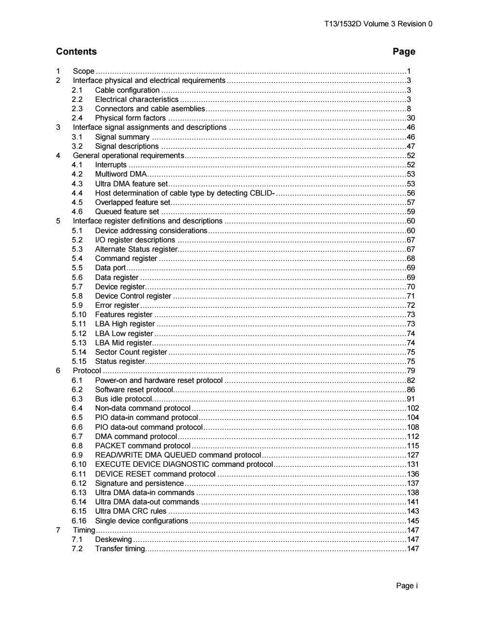
T13/1532D Volume 3 Revision 0 Page i Contents Page 1 Scope .....................................................................................................................................1 2 Interface physical and electrical requirements .............................................................................3 2.1 Cable configuration .........................................................................................................3 2.2 Electrical characteristics .................................................................................................3 2.3 Connectors and cable asemblies......................................................................................8 2.4 Physical form factors ......................................................................................................30 3 Interface signal assignments and descriptions ............................................................................46 3.1 Signal summary .............................................................................................................46 3.2 Signal descriptions .........................................................................................................47 4 General operational requirements...............................................................................................52 4.1 Interrupts .......................................................................................................................52 4.2 Multiword DMA...............................................................................................................53 4.3 Ultra DMA feature set......................................................................................................53 4.4 Host determination of cable type by detecting CBLID-........................................................56 4.5 Overlapped feature set.....................................................................................................57 4.6 Queued feature set .........................................................................................................59 5 Interface register definitions and descriptions ..............................................................................60 5.1 Device addressing considerations.....................................................................................60 5.2 I/O register descriptions ..................................................................................................67 5.3 Alternate Status register..................................................................................................67 5.4 Command register ..........................................................................................................68 5.5 Data port........................................................................................................................69 5.6 Data register ..................................................................................................................69 5.7 Device register................................................................................................................70 5.8 Device Control register ....................................................................................................71 5.9 Error register..................................................................................................................72 5.10 Features register ............................................................................................................73 5.11 LBA High register ...........................................................................................................73 5.12 LBA Low register............................................................................................................74 5.13 LBA Mid register.............................................................................................................74 5.14 Sector Count register......................................................................................................75 5.15 Status register................................................................................................................75 6 Protocol ..................................................................................................................................79 6.1 Power-on and hardware reset protocol ..............................................................................82 6.2 Software reset protocol....................................................................................................86 6.3 Bus idle protocol.............................................................................................................91 6.4 Non-data command protocol ............................................................................................102 6.5 PIO data-in command protocol.........................................................................................104 6.6 PIO data-out command protocol.......................................................................................108 6.7 DMA command protocol..................................................................................................112 6.8 PACKET command protocol ............................................................................................115 6.9 READ/WRITE DMA QUEUED command protocol..............................................................127 6.10 EXECUTE DEVICE DIAGNOSTIC command protocol.........................................................131 6.11 DEVICE RESET command protocol .................................................................................136 6.12 Signature and persistence...............................................................................................137 6.13 Ultra DMA data-in commands ..........................................................................................138 6.14 Ultra DMA data-out commands ........................................................................................141 6.15 Ultra DMA CRC rules ......................................................................................................143 6.16 Single device configurations .............................................................................................145 7 Timing.....................................................................................................................................147 7.1 Deskewing .....................................................................................................................147 7.2 Transfer timing................................................................................................................147
T13/1532D Volume 3 Revision 0 Tables Page 1 PACKET delivered command sets............... 2 2 DC characteristics..4 3 AC characteristics.... 4 Driver types and required termination...6 5 Typical series termination for Ultra DMA.....8 6 Host or device 40-pin I/O header.... 10 7 40-pin l/O cable connector................... 11 8 40-pin 1/O connector interface signals................. …12 9 40-conductor cable configuration......... 13 10 80-conductor cable electrical requirements......................... 4444444444444444440444444444444044 14 11 80-conductor ribbon cable.......... .14 12 80-conductor cable configuration...... .15 13 Signal assignments for connectors grounding even conductors 16 14 Signal assignments for connectors grounding odd conductors. 1 15 Device 4-pin power header. 19 164-pin power cable connector. 20 17 4-pin power connector pin assignments........ 20 18 Unitized connector... 22 19 Unitized connector... 22 20 50-pin connector....... 23 21 Signal assignments for 50-pin 2.5 inch form factor style connector 444444 24 22 Signal assignments for 68-pin connector..................... 26 23 1.8 inch 3.3V parallel connector............ 29 24 Pin assignments for the 1.8 inch 3.3V parallel connector............ 444444 30 25 3.5 inch form factor.............. 31 26 2.5 inch form factor.......... 34 272.5 inch form factor connector location.37 28 1.8 inch 5V parallel form factor.............. 39 29 1.8 inch 5V parallel form factor connector location 40 30 1.8 inch 3.3vparallel form factor. 42 31 5.25.inch HDD form factor...................... 43 32 5.25 inch CD-ROM form factor........... 44444 45 33 Interface signal name assignments............. 46 34 Cable type identification....... 50 35 Host detection of CBLID-... 44404444444404444044440444444440 57 36 Device repsonse to DOIW-/DOIR-....... 61 37 Device is not selected,DMACK-is not asserted................... 62 38 Device is selected,DMACK-is not asserted....63 39 Device is selected,DMACK-is asserted (for Multiword DMA only).... 64 40 Device 1 is selected and Device 0 is responding for Device 1........... 65 41 Device is in Sleep mode,DEVICE RESET is not implemented,DMACK-is not asserted.................. 6 42 Device is in Sleep mode,DEVICE RESET is implemented,DMACK-is not asserted.......................67 43 Equations for parallel generation of a CRC polynomial..... 145 44 Register transfer to/from device.149 45 PlO data transfer to/from device........................... 151 46 Multiword DMA data transfer.. 152 47 Ultra DMA data burst timing requirements.......... 157 48 Ultra DMA data burst timing descriptions. 158 49 Ultra DMA sender and recipient Ic timing requirements.......................................159 Figures Page Page ii
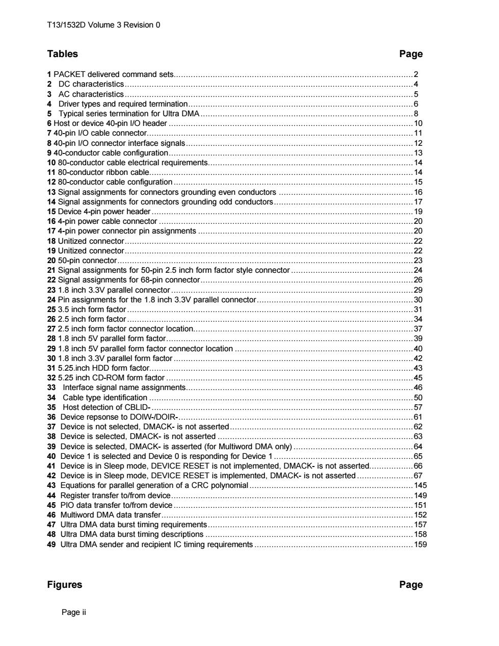
T13/1532D Volume 3 Revision 0 Page ii Tables Page 1 PACKET delivered command sets..................................................................................................2 2 DC characteristics......................................................................................................................4 3 AC characteristics......................................................................................................................5 4 Driver types and required termination............................................................................................6 5 Typical series termination for Ultra DMA.......................................................................................8 6 Host or device 40-pin I/O header ....................................................................................................10 7 40-pin I/O cable connector.............................................................................................................11 8 40-pin I/O connector interface signals.............................................................................................12 9 40-conductor cable configuration....................................................................................................13 10 80-conductor cable electrical requirements....................................................................................14 11 80-conductor ribbon cable............................................................................................................14 12 80-conductor cable configuration ..................................................................................................15 13 Signal assignments for connectors grounding even conductors .......................................................16 14 Signal assignments for connectors grounding odd conductors.........................................................17 15 Device 4-pin power header...........................................................................................................19 16 4-pin power cable connector ........................................................................................................20 17 4-pin power connector pin assignments ........................................................................................20 18 Unitized connector......................................................................................................................22 19 Unitized connector......................................................................................................................22 20 50-pin connector.........................................................................................................................23 21 Signal assignments for 50-pin 2.5 inch form factor style connector..................................................24 22 Signal assignments for 68-pin connector.......................................................................................26 23 1.8 inch 3.3V parallel connector...................................................................................................29 24 Pin assignments for the 1.8 inch 3.3V parallel connector................................................................30 25 3.5 inch form factor.....................................................................................................................31 26 2.5 inch form factor.....................................................................................................................34 27 2.5 inch form factor connector location..........................................................................................37 28 1.8 inch 5V parallel form factor.....................................................................................................39 29 1.8 inch 5V parallel form factor connector location .........................................................................40 30 1.8 inch 3.3V parallel form factor..................................................................................................42 31 5.25.inch HDD form factor............................................................................................................43 32 5.25 inch CD-ROM form factor .....................................................................................................45 33 Interface signal name assignments.............................................................................................46 34 Cable type identification ............................................................................................................50 35 Host detection of CBLID-...........................................................................................................57 36 Device repsonse to DOIW-/DOIR-................................................................................................61 37 Device is not selected, DMACK- is not asserted...........................................................................62 38 Device is selected, DMACK- is not asserted ................................................................................63 39 Device is selected, DMACK- is asserted (for Multiword DMA only).................................................64 40 Device 1 is selected and Device 0 is responding for Device 1 .........................................................65 41 Device is in Sleep mode, DEVICE RESET is not implemented, DMACK- is not asserted..................66 42 Device is in Sleep mode, DEVICE RESET is implemented, DMACK- is not asserted .......................67 43 Equations for parallel generation of a CRC polynomial ...................................................................145 44 Register transfer to/from device...................................................................................................149 45 PIO data transfer to/from device ..................................................................................................151 46 Multiword DMA data transfer.......................................................................................................152 47 Ultra DMA data burst timing requirements....................................................................................157 48 Ultra DMA data burst timing descriptions .....................................................................................158 49 Ultra DMA sender and recipient IC timing requirements .................................................................159 Figures Page
T13/1532D Volume 3 Revision 0 1 ATA document relationships.............. .1 2 Ultra DMA termination with pull-up or pull-down......... 8 3 Host or device 40-pin l/O header....... .10 4 40-pin 1/O cable connector... 5 40-pin l/O header mounting...... 11 .12 640-conductor cable configuration..13 7 80-conductor ribbon cable........ .14 8 80-conductor cable configuration............... .15 9 Connector labeling for even or odd conductor grounding ……….18 10 Device 4-pin power header....... .19 11 4-pin power cable connector................. 20 12 Unitized connector........... .21 14 50-pin 2.5 inch form factor style connector 23 15 1.8 inch 3.3V parallel connector..................... 29 17 2.5 inch form factor ............. .33 18 2.5 inch form factor mounting holes....................... .35 19 2.5 inch form factor connector location.. .36 20 1.8 inch 5V parallel form factor......... .38 21 1.8 inch 5V parallel form factor connector location............... .40 22 1.8 inch 3.3V parallel form factor.. .41 23 5.25 inch HDD form factor....... .43 24 5.25 inch CD-ROM form factor....... .44 25 5.25 inch CD-ROM connector location...... .45 26 Cable select example.......... .51 27 Alternate cable select example..................................... .52 28 Example configuration of a system with a 40-conductor cable............. .56 29 Example configuration of a system where the host detects a 40-conductor cable. .57 30 Example configuration of a system where the host detects an 80-conductor cable........................ .57 31 Overall host protocol state sequence.... .80 32 Overall device protocol state sequence. .81 33 Host power-on or hardware reset state diagram............82 34 Device power-on or hardware reset state diagram...... .83 35 Host software reset state diagram... .86 36 Device o software reset state diagram.. 88 37 Device 1 software reset state diagram...... .90 38 Host bus idle state diagram................... .92 39 Additional host bus idle state diagram with overlap or overlap and queuing..... .94 40 Device bus idle state diagram................. .97 41 Additional device bus idle state diagram with overlap or overlap and queuing. 4444444444444444444444 .99 42 Host non-data state diagram..... 103 43 Device non-data state diagram....... 103 44 Host Plo data-in state diagram..... .105 45 Device PIO data-in state diagram.... .107 46 Host PIO data-out state diagram...... .109 47 Device plo data-out state diagram... .111 48 Host DMA state diagram....................... .113 49 Device DMA state diagram............ .114 50 Host PACKET non-data and PIO data command state diagram... .116 51 Device PACKET non-data and PlO data command state diagram................................. .119 52 Host PACKET DMA command state diagram....... 122 53 Device PACKET DMA command state diagram.... 125 54 Host DMA QUEUED state diagram........... 128 55 Device DMA QUEUED command state diagram................ .130 56 Host EXECUTE DEVICE DIAGNOSTIC state diagram... 132 57 Device 0 EXECUTE DEVICE DIAGNOSTIC state diagram...... .133 Page ii
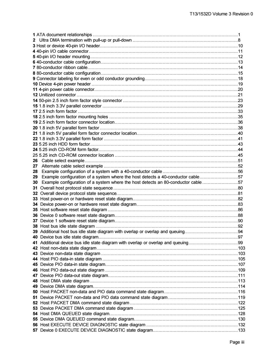
T13/1532D Volume 3 Revision 0 Page iii 1 ATA document relationships ..........................................................................................................1 2 Ultra DMA termination with pull-up or pull-down .............................................................................8 3 Host or device 40-pin I/O header.....................................................................................................10 4 40-pin I/O cable connector.............................................................................................................11 5 40-pin I/O header mounting............................................................................................................12 6 40-conductor cable configuration ....................................................................................................13 7 80-conductor ribbon cable..............................................................................................................14 8 80-conductor cable configuration ....................................................................................................15 9 Connector labeling for even or odd conductor grounding....................................................................18 10 Device 4-pin power header ...........................................................................................................19 11 4-pin power cable connector.........................................................................................................20 12 Unitized connector......................................................................................................................21 14 50-pin 2.5 inch form factor style connector ....................................................................................23 15 1.8 inch 3.3V parallel connector ...................................................................................................29 17 2.5 inch form factor .....................................................................................................................33 18 2.5 inch form factor mounting holes ..............................................................................................35 19 2.5 inch form factor connector location..........................................................................................36 20 1.8 inch 5V parallel form factor.....................................................................................................38 21 1.8 inch 5V parallel form factor connector location..........................................................................40 22 1.8 inch 3.3V parallel form factor ..................................................................................................41 23 5.25 inch HDD form factor............................................................................................................43 24 5.25 inch CD-ROM form factor......................................................................................................44 25 5.25 inch CD-ROM connector location ..........................................................................................45 26 Cable select example................................................................................................................51 27 Alternate cable select example ..................................................................................................52 28 Example configuration of a system with a 40-conductor cable .......................................................56 29 Example configuration of a system where the host detects a 40-conductor cable............................57 30 Example configuration of a system where the host detects an 80-conductor cable ..........................57 31 Overall host protocol state sequence ...........................................................................................80 32 Overall device protocol state sequence.........................................................................................81 33 Host power-on or hardware reset state diagram.............................................................................82 34 Device power-on or hardware reset state diagram..........................................................................83 35 Host software reset state diagram ...............................................................................................86 36 Device 0 software reset state diagram..........................................................................................88 37 Device 1 software reset state diagram..........................................................................................90 38 Host bus idle state diagram ........................................................................................................92 39 Additional host bus idle state diagram with overlap or overlap and queuing.......................................94 40 Device bus idle state diagram......................................................................................................97 41 Additional device bus idle state diagram with overlap or overlap and queuing....................................99 42 Host non-data state diagram .......................................................................................................103 43 Device non-data state diagram ....................................................................................................103 44 Host PIO data-in state diagram ...................................................................................................105 45 Device PIO data-in state diagram.................................................................................................107 46 Host PIO data-out state diagram .................................................................................................109 47 Device PIO data-out state diagram...............................................................................................111 48 Host DMA state diagram ............................................................................................................113 49 Device DMA state diagram..........................................................................................................114 50 Host PACKET non-data and PIO data command state diagram......................................................116 51 Device PACKET non-data and PIO data command state diagram ...................................................119 52 Host PACKET DMA command state diagram ...............................................................................122 53 Device PACKET DMA command state diagram ............................................................................125 54 Host DMA QUEUED state diagram..............................................................................................128 55 Device DMA QUEUED command state diagram............................................................................130 56 Host EXECUTE DEVICE DIAGNOSTIC state diagram ...................................................................132 57 Device 0 EXECUTE DEVICE DIAGNOSTIC state diagram..............................................................133
T13/1532D Volume 3 Revision 0 58 Device 1 EXECUTE DEVICE DIAGNOSTIC command state diagram.................................... 135 59 Host DEVICE RESET command state diagram.136 60 Device DEVICE RESET command state diagram..................... 137 61 Example parallel CRC generator.....145 62 Register transfer to/from device.148 63 PlO data transfer to/from device...150 64 Initiating a Multiword DMA data transfer...........153 65 Sustaining a Multiword DMA data transfer.. 154 66 Device terminating a Multiword DMA data transfer.............................................155 67 Host terminating a Multiword DMA data transfer........156 68 Initiating an Ultra DMA data-in burst......... 160 69 Sustained Ultra DMA data-in burst.................... 161 70 Host pausing an Ultra DMA data-in burst....... 162 71 Device terminating an Ultra DMA data-in burst 163 72 Host terminating an Ultra DMA data-in burst.......... 164 73 Initiating an Ultra DMA data-out burst.................... 165 74 Sustained Ultra DMA data-out burst..................... 166 75 Device pausing an Ultra DMA data-out burst.................. .167 76 Host terminating an Ultra DMA data-out burst..... .168 77 Device terminating an Ultra DMA data-out burst.... 169 Annexes Page A Device determination of cable type................ 170 B Signal integrity and UDMA implementation guide 173 C Register selection address summary..................... 227 Page iv
T13/1532D Volume 3 Revision 0 Page iv 58 Device 1 EXECUTE DEVICE DIAGNOSTIC command state diagram ..............................................135 59 Host DEVICE RESET command state diagram ............................................................................136 60 Device DEVICE RESET command state diagram..........................................................................137 61 Example parallel CRC generator..................................................................................................145 62 Register transfer to/from device...................................................................................................148 63 PIO data transfer to/from device ..................................................................................................150 64 Initiating a Multiword DMA data transfer.......................................................................................153 65 Sustaining a Multiword DMA data transfer...................................................................................154 66 Device terminating a Multiword DMA data transfer........................................................................155 67 Host terminating a Multiword DMA data transfer ..........................................................................156 68 Initiating an Ultra DMA data-in burst ............................................................................................160 69 Sustained Ultra DMA data-in burst ..............................................................................................161 70 Host pausing an Ultra DMA data-in burst .....................................................................................162 71 Device terminating an Ultra DMA data-in burst..............................................................................163 72 Host terminating an Ultra DMA data-in burst.................................................................................164 73 Initiating an Ultra DMA data-out burst ..........................................................................................165 74 Sustained Ultra DMA data-out burst ............................................................................................166 75 Device pausing an Ultra DMA data-out burst.................................................................................167 76 Host terminating an Ultra DMA data-out burst...............................................................................168 77 Device terminating an Ultra DMA data-out burst............................................................................169 Annexes Page A Device determination of cable type................................................................................................170 B Signal integrity and UDMA implementation guide ...........................................................................173 C Register selection address summary ............................................................................................227