
Inputs Output y L H L H H y H L H HH Fig.10-1 Positive Logic NAND Gate 2002 Prentice Hall.Inc. M.Morris Mano DIGITAL DESIGN,3e

Inputs Output x y LL H L H L H L L HH L Fig.10-2 Positive Logic NOR Gate 2002 Prentice Hall,Inc. M.Morris Mano DIGITAL DESIGN,3e
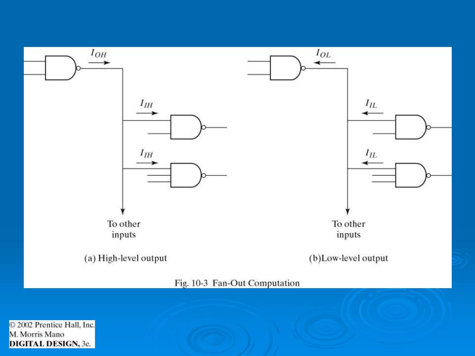
11L To other To other inputs inputs (a)High-level output (b)Low-level output Fig.10-3 Fan-Out Computation 2002 Prentice Hall.Inc. M.Morris Mano DIGITAL DESIGN,3e
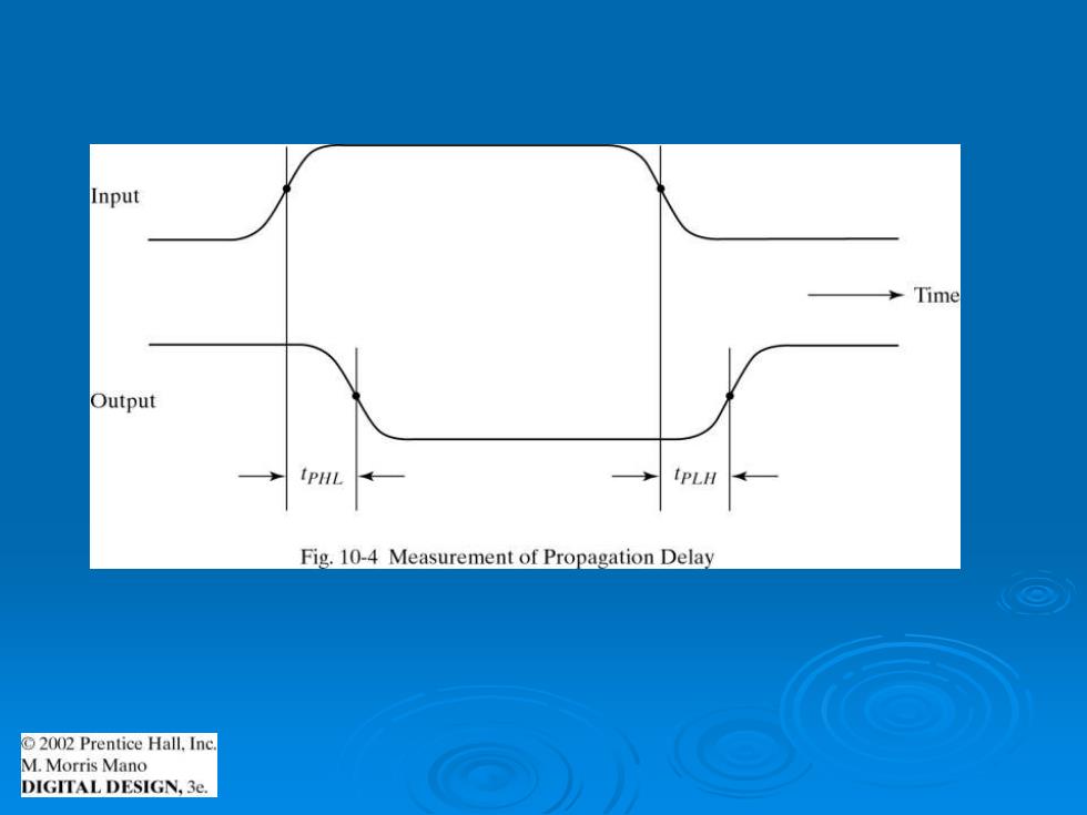
Input Time Output IPHL IPLH Fig.10-4 Measurement of Propagation Delay 2002 Prentice Hall.Inc M.Morris Mano DIGITAL DESIGN,3e
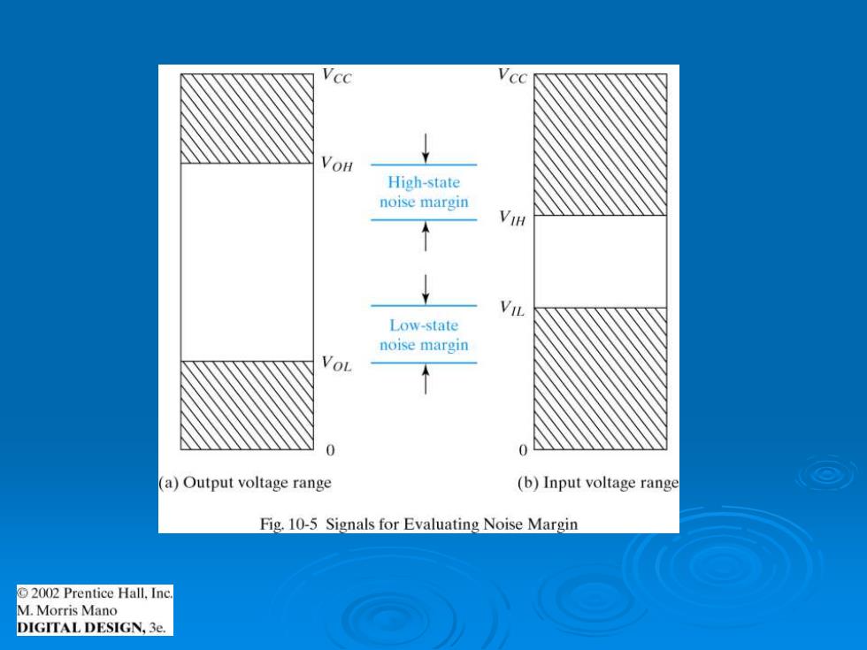
VOH High-state noise margin VIH VIL Low-state noise margin VOL 0 (a)Output voltage range (b)Input voltage range Fig.10-5 Signals for Evaluating Noise Margin 2002 Prentice Hall,Inc M.Morris Mano DIGITAL DESIGN,3e