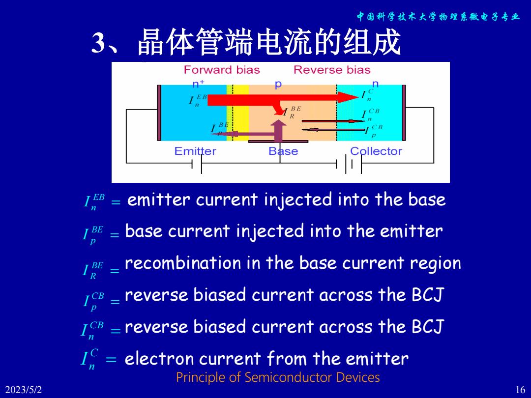
中国科学技术大学物理系微电子专业 3、晶体管端电流的组成 Forward bias Reverse bias n+ Emitter Base Collector 1.emitter current injected into the base base current injected into the emitter 1-recombination in the base current region reverse biased current across the BCJ reverse biased current across the BCJ I electron current from the emitter Principle of Semiconductor Devices 2023/5/2 16
中国科学技术大学物理系微电子专业 2023/5/2 Tuesday 16 emitter current injected into the base base current injected into the emitter recombination in the base current region reverse biased current across the BCJ reverse biased current across the BCJ electron current from the emitter EB n I BE p I BE R I CB p I CB n I C n I 3、晶体管端电流的组成 Principle of Semiconductor Devices

中国科学技术大学物理系微电子专业 4、晶体管的电流增益 直流共基极电流放大系数(或电流增益)的定义 为 其中, 发射效率: En 基区传输因子 aT= do =yaT Principle of Semiconductor Devices 2023/5/2 17
中国科学技术大学物理系微电子专业 2023/5/2 Tuesday 17 4、 晶体管的电流增益 • 直流共基极电流放大系数(或电流增益)的定义 为 其中, 发射效率: 基区传输因子 Ep Cp Ep En Ep Ep En Cp E Cp I I I I I I I I I I 0 0 , Ep En Ep E Ep I I I I I Ep Cp T I I T 0 Principle of Semiconductor Devices
中国科学技术大学物理系微电子考业 集电极电流表达式: Ic dolg+cBo 下标CB:表示C和B结的端电流,O:表示 对应的第三端与第二端之间为开态。 共发射极晶体管的电流放大系数(电流增 益)为: 1-a。1g-1cp1cn+18 Principle of Semiconductor Devices 2023/5/2 18
中国科学技术大学物理系微电子专业 2023/5/2 Tuesday 18 集电极电流表达式: 下标CB: 表示C和B结的端电流,O: 表示 对应的第三端与第二端之间为开态。 C E CBO I I I 0 • 共发射极晶体管的电流放大系数(电流增 益)为 : Cn B Cp E Cp Cp I I I I I I 0 0 0 1 Principle of Semiconductor Devices

中国科学技术大学物理系微电子专业 共发射级晶体管放大 a E Principle of Semiconductor Devices 2023/5/2 19
中国科学技术大学物理系微电子专业 2023/5/2 Tuesday 19 共发射级晶体管放大 IB IC IE Principle of Semiconductor Devices

中国科学技术大学物理系微电子专业 IC IE IC IB IB 0 VCE VCE VBE VCB VCB IB VBE IE 永IC 0 (c) 晶体管的三种连接法(a)共基极、 (b)共发 射极和(c)共集电极 电路应用中,晶体管的共发射级接法 最常用,即发射极作为公共端,基极 和集电极为输入和输出端。 Principle of Semiconductor Devices 2023/5/2 20
中国科学技术大学物理系微电子专业 2023/5/2 Tuesday 20 晶体管的三种连接法 (a)共基极、 (b)共发 射极和(c)共集电极 (a) (b) (c) • 电路应用中,晶体管的共发射级接法 最常用,即发射极作为公共端,基极 和集电极为输入和输出端。 Principle of Semiconductor Devices